94
CHAPTER 4 External Bus Interface
4.5.2 Area Mode Register 1 (AMD1)
The area mode register 1 (AMD1) specifies the memory access operation mode for each
chip select area.
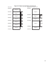
■ Area Mode Register 1 (AMD1)
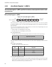
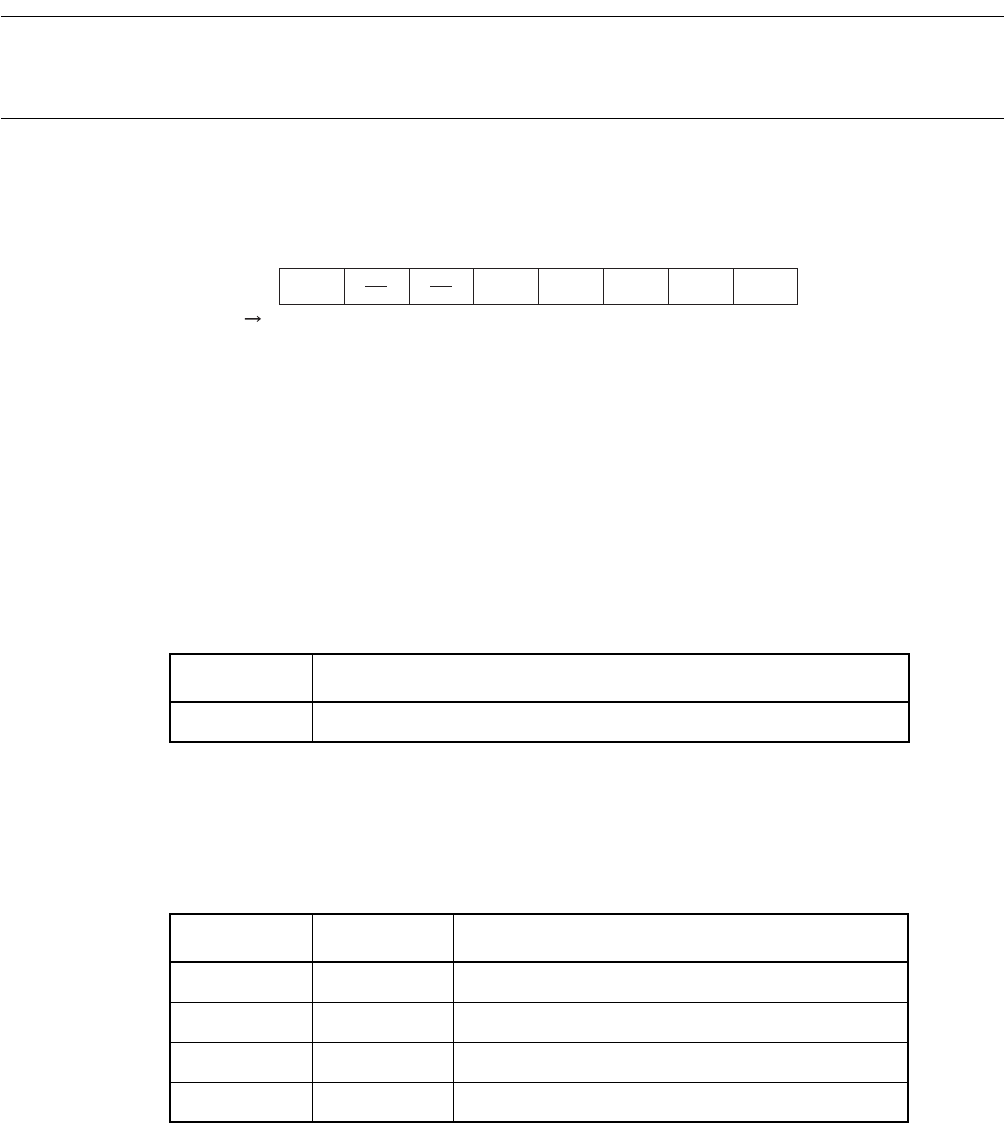
Figure 4.5-5 Area mode register 1 (AMD1)
The area mode register 1 (AMD1) specifies the operation mode for the chip select area 1 (the area specified
by ASR1 and AMR1). In area 1, the time division input/output interface can be specified for the address/
data input/output.
The time division input/output interface outputs addresses to the data bus and inputs/outputs data, and
supports 8-bit and 16-bit bus widths only as follows.
• 8-bit bus width: A7 to A0 multiplexes to D31 to D24.
• 16-bit bus width: A15 to A0 multiplexes to D31 to D16.
[bit7] :MPX (MultiPleX bit)
The MPX controls the time division input/output interface for the address and data input/output.
When the external bus mode is used for this product, the time division input/output interface must be
specified.
[bit4, 3] :BW1, 0 (Bus Width bit)
The BW1 and 0 specifies the bus width of area 1.
[bit2 to 0] :WTC2 to 0(Wait Cycle bit)
The WTC specifies the auto insert wait cycle number for normal bus interface and time division input/
output interface operation. Operation is the same as WTC2 to WTC0 of the AMD0, but is initialized to
"000" by reset, and the insert wait cycle number will be "0".
76543210
Initial value
Address: 0000 0621
H BW1 BW0 WTC2 WTC1 WTC0 0--00000B
R/W
MPX
R/WR/WR/WR/WR/W
bit
Access
0 Specification prohibited
1 Time division input/output interface
BW1 BW0 Bus width
0 0 8 bits
0 1 16 bits
1 0 reserved
1 1 reserved


