


19
●
Latch up
The semiconductor device is composed by the formation of the region of the P-type and the N-type on the
substrate. Internal parasitism PN junction (thyristor structure) might keep doing on-line when the voltage of
an external abnormal voltage is added, and the heavy-current which exceeds hundreds of mA flow to the
power supply terminal. This is called a latch up. The reliability of the device is not only damaged when this
phenomenon occurs but also there is dreading the arrival heat generation, smoking, and the ignition to
destruction. Please note the following points to prevent this.
• There must not be what the voltage more than the maximum rating adds the terminal. Please note
abnormal noise and surge etc.
• An abnormal current must not flow in consideration of the power supply turning on sequence.
●
Restriction of safety etc. and observance of standard
All over the world, various restrictions and standards of safety and the EMI, etc. have been installed. Please
suit these restriction and standard when the customer designs the equipment.
●
Fail safe design
The semiconductor device breaks down at a certain probability. The customer safely designs such as the
device redundancy, fire spreading prevention, exceeding current prevention, and prevention of malfunction
not to occur the injury accident, fire accident, and social damage consequently when the semiconductor
device is broken.
●
Attention concerning usage
The our company semiconductor device is intended to be used for a standard usage (associated equipment
for office appliances such as computers/OA and industries/communications/the measurements and
personal/home equipment etc.). The customer concerns the usage of threatening the life by the breakdown
and malfunction, dreading the damage to the human body, or the special application which the extreme
high reliability is requested (fro aviation/space, atomic control, device for relayed the bottom of the sea,
running control, the medical device to keep the life, etc.), be sure to consult with the sales division of our
company. When you use without the consultation and acknowledge that the responsibility cannot be
assumed about the occurring damage etc.
■ Precautions when Mounting Package
In the package, there are a lead insertion type and a surface mounting type. In both cases, quality assurance
for heat resistance at the soldering stage only applies to the mounting under conditions recommended by us.
Please inquire the section in charge of sales of our company about details of the mounting condition.
●
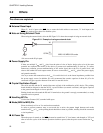
Lead insertion type
There are two ways to mount the lead insertion type package onto the printing board-the first is to directly
solder it onto the printing board, and the second is to mount it on the printing board using the socket.
When soldering it directly to the printing board, the flow soldering method (wave soldering method)
whereby the solder is melted after inserting the lead through the hole in the printing board is generally used.
In this case, heat stress in excess of the usual maximum rating preservation temperature is added to the lead
part at the soldering stage. Please mount under the mounting recommendation condition of our company.
When the mounting method using the socket is used, if surface processing of the socket contact point and
surface processing of the IC lead are different, contact failure may be generated after a prolonged period.
Therefore, checking the surface processing of the socket contact and surface processing of the IC lead is
recommended before mounting.