


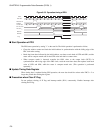
182
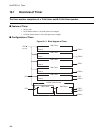
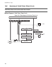
CHAPTER 9 Real Timing Generator (RTG)
This bit exists with the RTG0 only, and it affects the timing accuracy of all RTGs.
[bit2]:CLR
It is FIFO initialization bit.
The read value of this bit is always "0".
[bit1]:FUL
It is FIFO full flag.
[bit0]:EMP
It is FIFO empty flag.
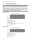
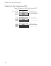
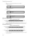
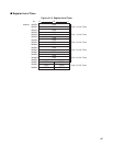
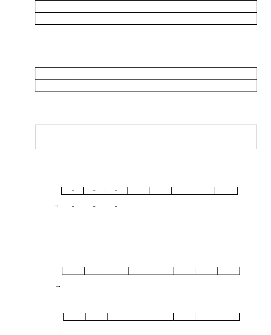
■ Output Data Register (RTGxD)
Figure 9.2-2 Output data register (RTGxD)
Data written to this register will be the RTG output data. Reading value is read that the RTG is current
output data. In terms of the RTG output, the value logically added (OR) per bit of each channel is output.
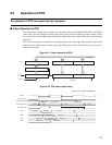
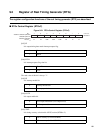
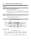
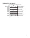
■ Timing Data Register (RTGxT)
Figure 9.2-3 Timing data register (RTGxT)
It is a register to set the output time of the RTG output. Writing this register sets the value set by the output
data register in FIFO format.
0 None
1 Clear FIFO.
0 FIFO empty status
1 FIFO full status
0 Data is remained in FIFO
1 FIFO empty status
7 6 5 4 3 2 1 0
---X XXXX
B
Initial value
bit
Address: 000035
H
(RTG0D)
000039
H
(RTG1D)
00003D
H
(RTG2D)
R/W R/W R/W R/W
OD3 OD2 OD1 OD0
R/W
OD4
Access
7 6 5 4 3 2 1 0
XXXX XXXX
B
Initial value
bit
Address: 000036H (RTG0TH)
00003A
H (RTG1TH)
00003E
H (RTG2TH)
WWWWWWWW
D15 D14 D13 D12 D11 D10 D09 D08
Access
7 6 5 4 3 2 1 0
XXXX XXXX
B
Initial value
bit
Address: 000037
H
(RTG0TL)
00003B
H
(RTG1TL)
00003F
H
(RTG2TL)
WWWWWWWW
D07 D06 D05 D04 D03 D02 D01 D00
Access