


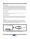

S3F80JB CLOCK CIRCUITS
7-3
SYSTEM CLOCK CONTROL REGISTER (CLKCON)
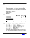
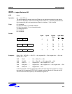
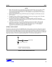
The system clock control register, CLKCON, is located in address D4H, Set1, Bank0. It is read/write addressable
and has the following functions:
— Oscillator frequency divide-by value
The CLKCON.7 - .5 and CLKCON.2- .0 Bit are not used in S3F80JB. After a reset, the main oscillator is activated,
and the f
OSC/16
(the slowest clock speed) is selected as the CPU clock. If necessary, you can then increase the
CPU clock speed to f
OSC
, f
OSC/2
, f
OSC/8
or f
OSC/16
.
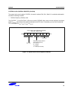
System Clock Control Register (CLKCON)
D4H, Set 1, Bank 0, R/W
.7 .6 .5 .4 .3 .2 .1 .0MSB LSB
Not used
Divide-by selection bits for
CPU clock frequency
00 = fosc/16
01 = fosc/8
10 = fosc/2
11 = fosc (non-divided)
Not used
Figure 7-4. System Clock Control Register (CLKCON)