


RESET S3F80JB
8-4
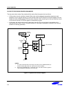
RESET MECHANISM
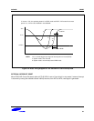
The interlocking work of reset pin and LVD circuit supplies two operating modes: back-up mode input, and system
reset input. Back-up mode input automatically creates a chip stop state when the reset pin is set to low level or
the voltage at V
DD
is lower than V
LVD
. When the reset pin is at a high state and the LVD circuit detects rising edge
of V
DD
on the point V
LVD
, the reset pulse generator makes a reset pulse, and system reset occurs. When the
operating mode is in STOP mode and IPOR / LVD control bit of smart option is ‘0’, the LVD circuit is disabled to
reduce the current consumption under 6uA instead of 20uA (at V
DD
= 3.6 V). Therefore, although the voltage at
V
DD
is lower than V
LVD
, the chip doesn’t go into back-up mode when the operating state is in stop mode and reset
pin is High level (Vreset > V
IH
).
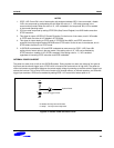
EXTERNAL RESET PIN
When the nRESET pin transiting from V
IL
(low input level of reset pin) to V
IH
(high input level of reset pin), the
reset pulse is generated on the condition of “V
DD
≥ V
LVD
“.
WATCH DOG TIMER RESET
The watchdog timer that can recover to normal operation from abnormal function is built in S3F80JB. Watchdog
timer generates a system reset signal, if Basic Timer Counter (BTCNT) isn’t cleared within a specific time by
program. For more understanding of the watchdog timer function, please see the chapter 11, Basic Timer and
Timer0.
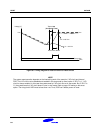
LVD RESET
The Low Voltage Detect Circuit (LVD) is built on the S3F80JB product to generate a system reset when
IPOR/LVD Control Bit of smart option is set to ‘1’ regardless of operation mode. So if IPOR / LVD Control Bit of
smart option is set to ‘1’ and the operating status is stop mode, LVD can make a system reset. When the voltage
at V
DD
is falling down and passing V
LVD
, the chip go into back-up mode at the moment “V
DD
= V
LVD
”. And the
voltage at V
DD
is rising up, the reset pulse is occurred at the moment “V
DD
≥ V
LVD
“.
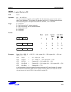
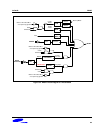
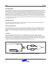
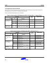
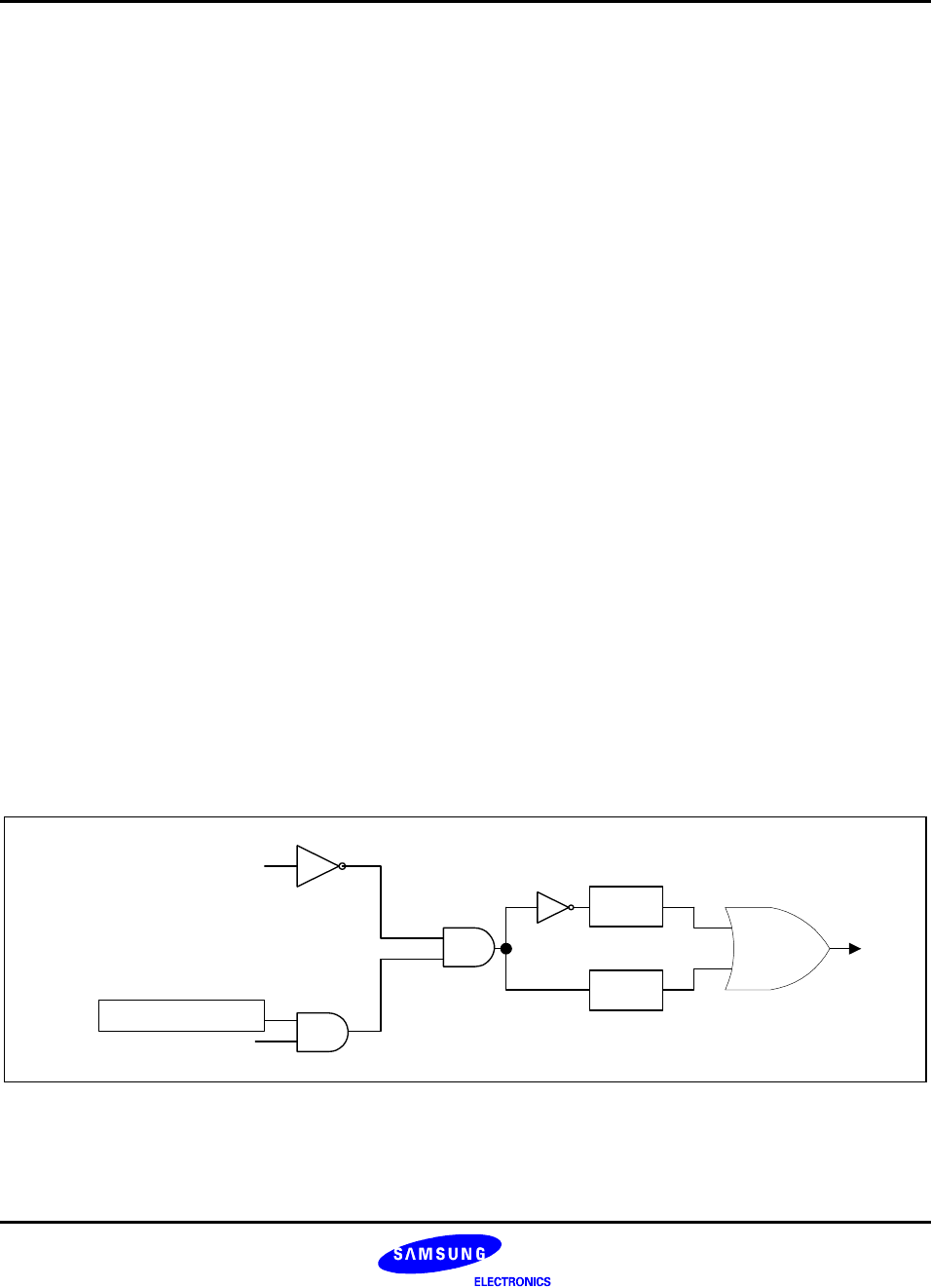
STOP Instruction
Reset
IPOR / LVD Control Bit:
smart option bit[7] @03FH (
note 1
)
LVD
IPOR
STOPCON
(note 2)
(
note3
)
(
note4
)
Figure 8-3. RESET Block Diagram by LVD for The S3F80JB in Stop Mode