


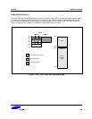
S3F80JB ADDRESS SPACES
2-5
REGISTER ARCHITECTURE
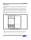
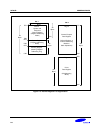
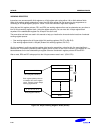
In the S3F80JB implementation, the upper 64-byte area of register files is expanded two 64-byte areas, called set
1 and set 2. The upper 32-byte area of set 1 is further expanded two 32-byte register banks (bank 0 and bank 1),
and the lower 32-byte area is a single 32-byte common area.
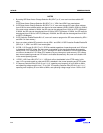
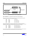
In case of S3F80JB the total number of addressable 8-bit registers is 333. Of these 333 registers, 22 bytes are for
CPU and system control registers, 39 bytes are for peripheral control and data registers, 16 bytes are used as
shared working registers, and 272 registers are for general-purpose use.
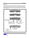
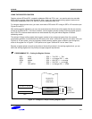
The extension of register space into separately addressable areas (sets, banks) is supported by various
addressing mode restrictions: the select bank instructions, SB0 and SB1.
Specific register types and the area occupied in the S3F80JB internal register space are summarized in Table 2-
1.
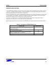
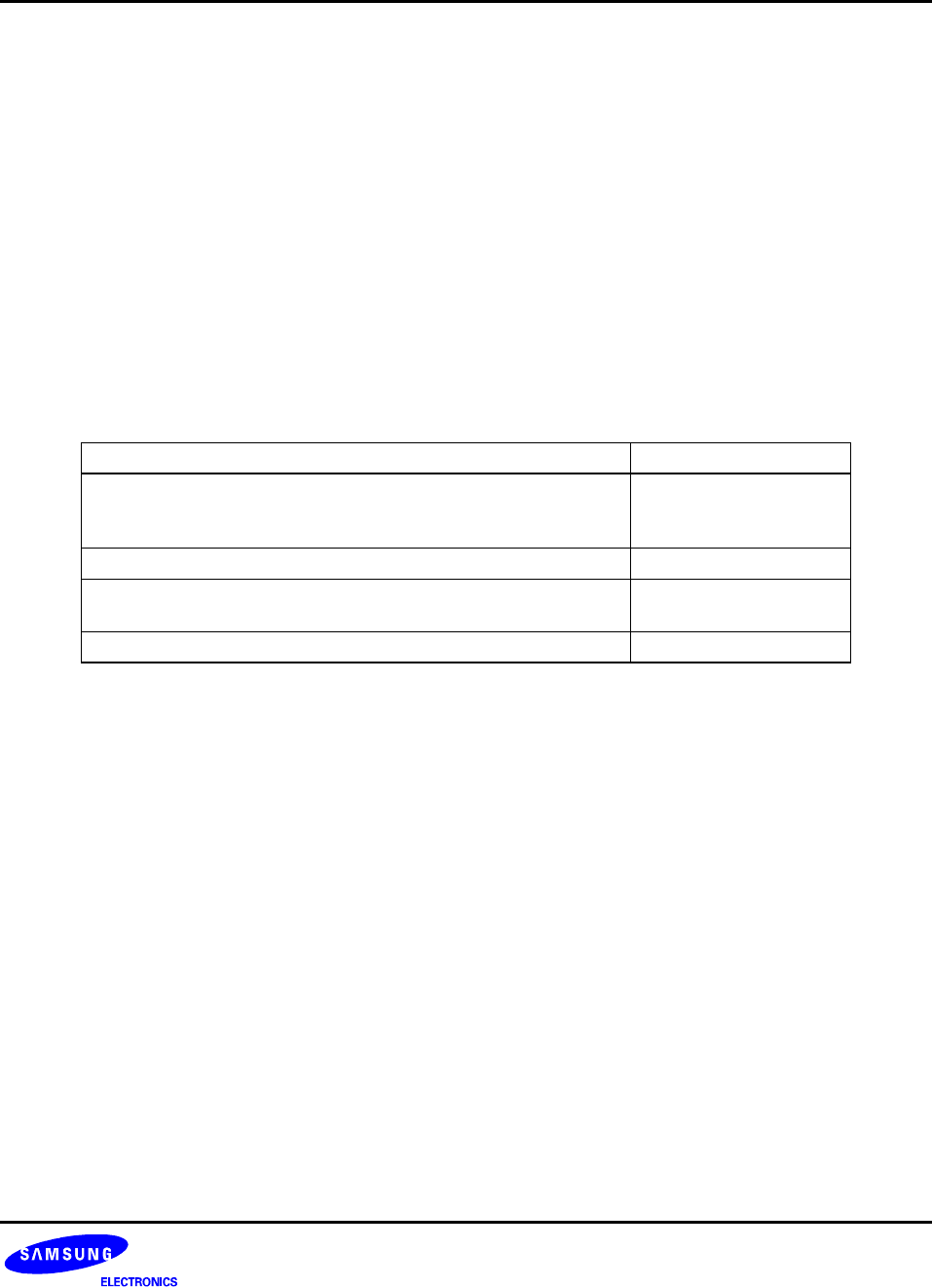
Table 2-1. The Summary of S3F80JB Register Type
Register Type Number of Bytes
General-purpose registers (including the 16-byte common
working register area, the 64-byte set 2 area and 192-byte prime
register area of page 0)
272
CPU and system control registers 22
Mapped clock, peripheral, and I/O control and data registers
(bank 0: 27 registers, bank 1: 12 registers)
39
Total Addressable Bytes 333