


CONTROL REGISTERS S3F80JB
4-20
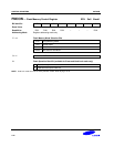
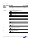
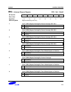
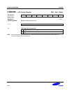
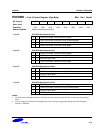
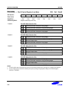
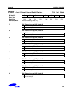
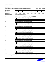
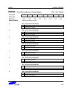
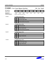
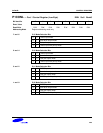
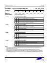
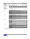
P0CONL — Port 0 Control Register (Low Byte) E9H Set1 Bank0
Bit Identifier .7 .6 .5 .4 .3 .2 .1 .0
Reset Value
0 0 0 0 0 0 0 0
Read/Write
R/W R/W R/W R/W R/W R/W R/W R/W
Addressing Mode
Register addressing mode only
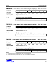
.7 and .6 P0.3/INT3 Mode Selection Bits
0 0 C-MOS input mode; interrupt on falling edges
0 1 C-MOS input mode; interrupt on rising and falling edges
1 0 Push-pull output mode
1 1 C-MOS input mode; interrupt on rising edges
.5 and .4 P0.2/INT2 Mode Selection Bits
0 0 C-MOS input mode; interrupt on falling edges
0 1 C-MOS input mode; interrupt on rising and falling edges
1 0 Push-pull output mode
1 1 C-MOS input mode; interrupt on rising edges
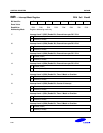
.3 and .2 P0.1/INT1 Mode Selection Bits
0 0 C-MOS input mode; interrupt on falling edges
0 1 C-MOS input mode; interrupt on rising and falling edges
1 0 Push-pull output mode
1 1 C-MOS input mode; interrupt on rising edges
.1 and .0 P0.0/INT0 Mode Selection Bits
0 0 C-MOS input mode; interrupt on falling edges
0 1 C-MOS input mode; interrupt on rising and falling edges
1 0 Push-pull output mode
1 1 C-MOS input mode; interrupt on rising edges
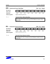
NOTES:
1. The INT3–INT0 external interrupts at P0.3–P0.0 are interrupt level IRQ6. Each interrupt has a separate vector address.
2. You can assign pull-up resistors to individual port 0 pins by making the appropriate settings to the P0PUR register.
(P0PUR.3 – P0PUR.0)