


CONTROL REGISTERS S3F80JB
4-26
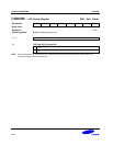
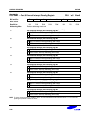
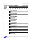
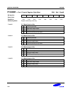
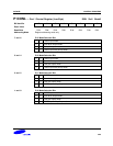
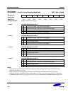
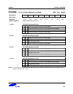
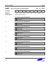
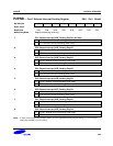
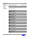
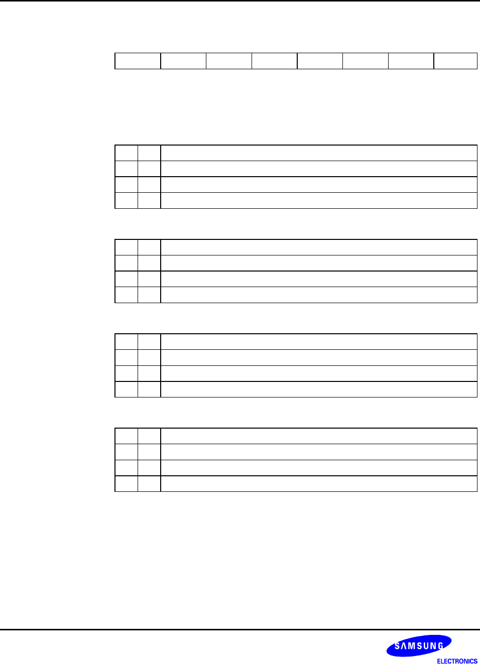
P2CONH — Port 2 Control Register (High Byte) ECH Set1 Bank0
Bit Identifier .7 .6 .5 .4 .3 .2 .1 .0
Reset Value
0 0 0 0 0 0 0 0
Read/Write
R/W R/W R/W R/W R/W R/W R/W R/W
Addressing Mode
Register addressing mode only
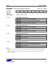
.7 and .6 P2.7/INT9 Mode Selection Bits
0 0 C-MOS input mode; interrupt on falling edges
0 1 C-MOS input mode; interrupt on rising and falling edges
1 0 Push-pull output mode
1 1 C-MOS input mode; interrupt on rising edges
.5 and .4 P2.6/INT9 Mode Selection Bits
0 0 C-MOS input mode; interrupt on falling edges
0 1 C-MOS input mode; interrupt on rising and falling edges
1 0 Push-pull output mode
1 1 C-MOS input mode; interrupt on rising edges
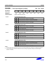
.3 and .2 P2.5/INT9 Mode Selection Bits
0 0 C-MOS input mode; interrupt on falling edges
0 1 C-MOS input mode; interrupt on rising and falling edges
1 0 Push-pull output mode
1 1 C-MOS input mode; interrupt on rising edges
.1 and .0 P2.4/INT9 Mode Selection Bits
0 0 C-MOS input mode; interrupt on falling edges
0 1 C-MOS input mode; interrupt on rising and falling edges
1 0 Push-pull output mode
1 1 C-MOS input mode; interrupt on rising edges
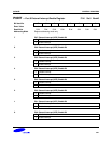
NOTES:
1. Pull-up resistors can be assigned to individual port2 pins by making the appropriate settings to the P2PUR control
register, location EEH, set 1, bank0.
2. Analog comparator inputs (CIN0-CIN3) for P2.4-P2.7 can be assigned to individual port 2 pins by making the
appropriate settings to the CMPSEL register, location EBH, set 1, bank1. If an analog comparator input is selected by
the CMPSEL register, normal I/O inputs for P2.4-P2.7 are disconnected regardless of P2CONH register’s setting value.