


S3F80JB
1
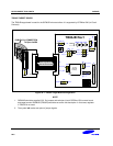
TOOL PROGRAMMING OF S3F80JB
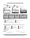
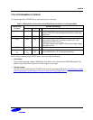
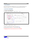
To read/write/erase by OTP/MTP writer, the following six pins are used.
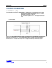
Table 1. Descriptions of Pins Used to Read/Write/Erase the Flash in Tool Program Mode
During Programming
Normal Chip
Pin Name
Pin Name Pin No. I/O Function
P3.0 SDAT 3[30] I/O Serial data pin. Output port when reading and input port when
writing. SDAT (P3.0) can be assigned as an input or push-pull
output port.
P3.1 SCLK 4[31] I Serial clock pin. Input only pin.
TEST TEST 9[4] I
Tool mode selection when TEST pin sets Logic value ‘1’. If
user uses the flash writer tool mode (ex.spw2+ etc.), user
should connect TEST pin to V
DD.
(S3F80JB supplies high voltage 12.5V by internal high voltage
generation circuit.)
NRESET nRESET 12[7] I Chip Initialization
V
DD
,
V
SS
V
DD
,
V
SS
5[32],
6[1]
– Power supply pin for logic circuit.
V
DD
should be tied to +3.3 V during programming.
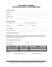
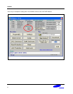
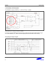
When writing or erasing using OTP/MTP writer, user must check the following:
— Vdd Voltage
The maximum operating voltage of S3F80JB is 3.6V. (Refer to the electrical data of S3F80JB manual.) The
selection flag of Vdd must be set to 3.3V as like a figure on next page.
— Test Pin Voltage
The TEST pin on socket board for OTP/MTP writer must be connected to Vdd (3.3V). The TEST pin on socket
board must not be connected Vpp(12.5V) which is generated from OTP/MTP Writer. So the specific socket
board for S3F80JB must be used, when writing or erasing using OTP/MTP writer.