


CONTROL REGISTERS S3F80JB
4-32
NOTES:
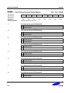
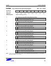
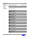
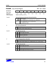
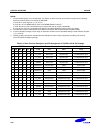
1. The port 3 data register, P3, at location E3H, set1, bank0, contains seven bit values which correspond to the following
Port 3 pin functions (bit 6 is not used for the S3F80JB:
a. Port3, bit 7: carrier signal on (“1”) or off (“0”).
b. Port3, bit 1,0: P3.1/REM/T0CK pin, bit 0: P3.0/T0PWM/T0CAP/T1CAP pin.
c. Port3, bit 3,2: P3.3, P3.2 are selected only to input pin with pull up resistor automatically.
d. Port3, bit 5,4: P3.5, P3.4 are selected into digital I/O by setting P345CON register at E1H, Set1, Bank1.
2. The alternative function enable/disable are enabled in accordance with function selection bit (bit5 and bit2).
3. In case of 42/44pin package, the pin assign for alternative functions can be selectable relating to mode selection bit (bit0,
1, 2, 3, 4 and 5)
4. Following Table is the specific example about the alternative function and pin assignment according to the each bit
control of P3CON in 42/44pin package.
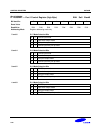
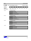
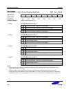
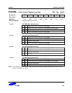
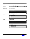
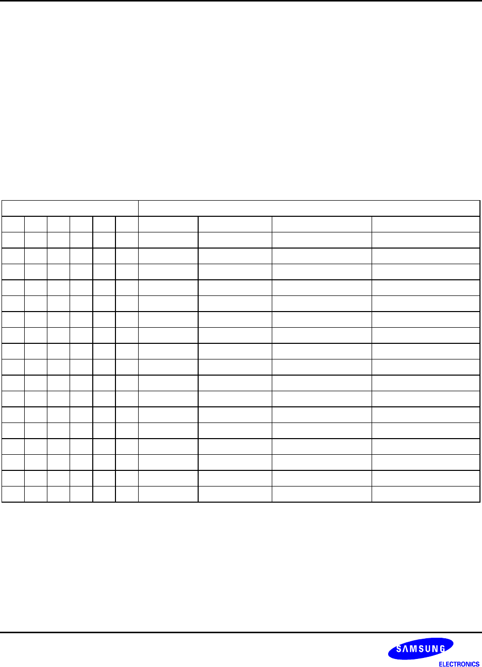
Table 4-3. Each Function Description and Pin Assignment of P3CON in 42/44 Pin Package
P3CON Each Function Description and Assignment to P3.0–P3.3
B5 B4 B3 B2 B1 B0 P3.0 P3.1 P3.2 P3.3
0 x x 0 x x Normal I/O Normal I/O Normal Input Normal Input
0 x x 1 0 0 T0_CAP Normal I/O Normal Input T1CAP/Normal Input
0 x x 1 1 1 T0_CAP Normal I/O Normal Input T1CAP/Normal Input
0 x x 1 0 1 T0PWM Normal I/O Normal Input T1CAP/Normal Input
0 x x 1 1 0 T0PWM Normal I/O Normal Input T1CAP/Normal Input
1 0 0 0 x x Normal I/O Normal Input T0CK Normal Input
1 1 1 0 x x Normal I/O Normal Input T0CK Normal Input
1 0 1 0 x x Normal I/O REM T0CK Normal Input
1 1 0 0 x x Normal I/O REM T0CK Normal Input
1 0 0 1 0 0 T0_CAP Normal Input T0CK/Normal Input T1CAP/Normal Input
1 1 1 1 1 1 T0_CAP Normal Input T0CK/Normal Input T1CAP/Normal Input
1 0 1 1 0 1 T0PWM REM T0CK/Normal Input T1CAP/Normal Input
1 1 0 1 1 0 T0PWM REM T0CK/Normal Input T1CAP/Normal Input
1 0 0 1 0 1 T0PWM Normal Input T0CK/Normal Input T1CAP/Normal Input
1 1 1 1 1 0 T0PWM Normal Input T0CK/Normal Input T1CAP/Normal Input
1 0 1 1 0 0 T0_CAP REM T0CK/Normal Input T1CAP/Normal Input
1 1 0 1 1 1 T0_CAP REM T0CK/Normal Input T1CAP/Normal Input