


RESET S3F80JB
8-6
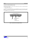
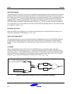
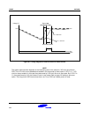
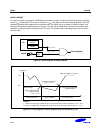
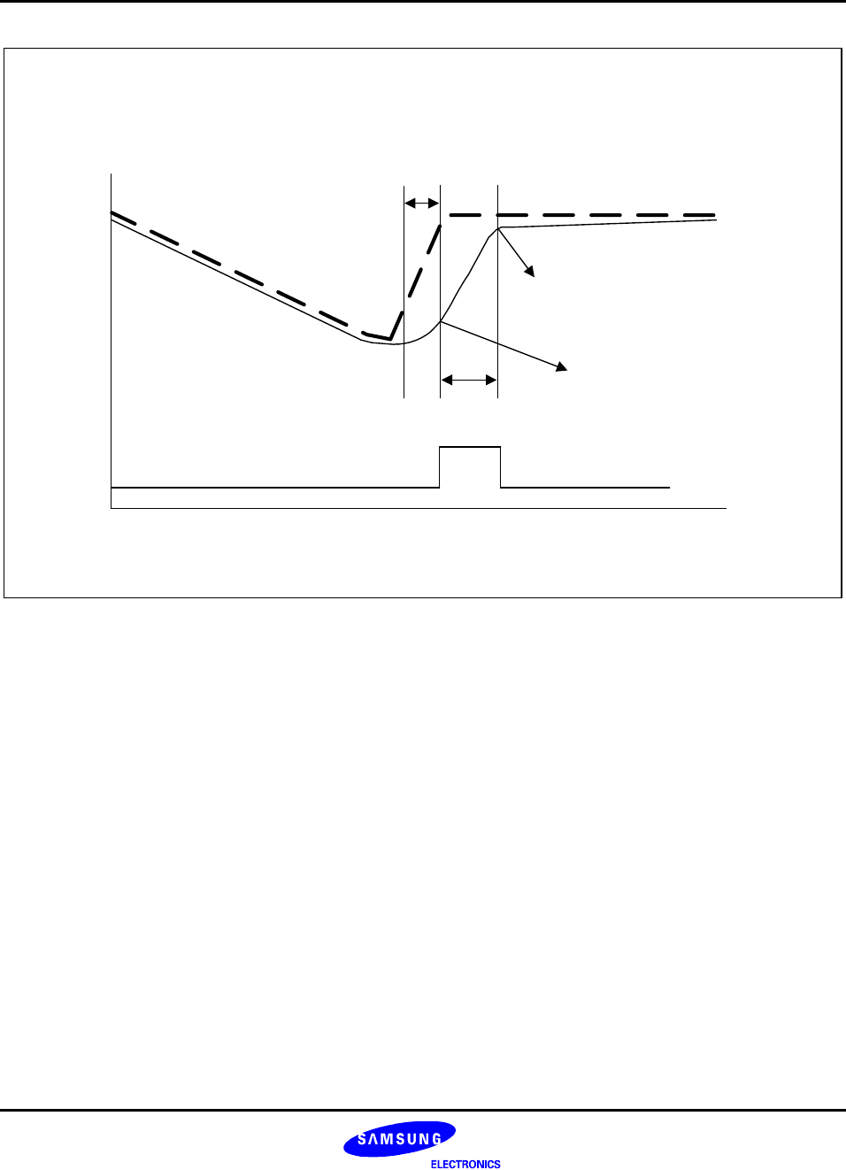
Voltage [V]
Time
Reset pulse
Va
Reset Pulse Width
V
DD
V
IH
= 0.85 V
DD
V
IL
= 0.4 V
DD
T
VDD
= 1ms
(V
DD
Rising Time)
V
DD
Figure 8-5. Timing Diagram for Internal Power-On Reset Circuit
NOTE
The system reset operation depends on the interlocking work of the reset pin, LVD circuit and Internal
POR. The LVD circuit can be disabled and enabled in the stop mode by smart option. If 3FH.7 is ‘1’, LVD
circuit is always enabled. In this case the system reset by LVD circuit occurs in stop mode. But, if 3FH.7 is
‘0’, the system reset by LVD circuit doesn’t occur in stop mode. Refer to page 2-3 relating to the smart
option. The rising time of VDD must be less than 1ms. If not, IPOR can’t detect power on reset.