


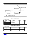


S3F80JB ELECTRICAL DATA (8MHz)
18-13
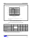
Minimun Instruction
Clock
1kHz
f
OSC
(Main Oscillator Frequency)
12345
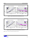
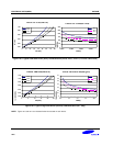
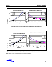
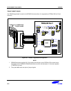
Supply Voltage (V)
Minimun Instruction Clock = 1/4n x oscillator frequency (n = 1, 2, 8, or 16)
A: 1.95 V, 8 MHz
250 kHz
1MHz
1.5MHz
2 MHz
8 MHz
6 MHz
4 MHz
400 kHz
67
500 kHz
A
1 MHz
2 MHz
Figure 18-12. Operating Voltage Range of S3F80JB
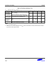
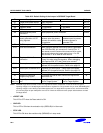
Table 18-10. AC Electrical Characteristics for Internal Flash ROM
(T
A
= –25 °C to + 85 °C)
Parameter Symbol Conditions Min Typ Max Unit
Flash Erase/Write/Read Voltage Fewrv
V
DD
1.95 3.3 3.6 V
Programming Time
(1)
Ftp 32 – 60
µS
Sector Erasing Time
(2)
Ftp1 10 – 20 mS
Chip Erasing Time
(3)
Ftp2
50 – 100 mS
Data Access Time
Ft
RS
V
DD
= 2.0 V
– 250 – nS
Number of Writing/Erasing FNwe – 10,000 – – Times
Data Retention Ftdr – 10 – – Years
1. The programming time is the time during which one byte (8-bit) is programmed.
2. The Sector erasing time is the time during which all 128-bytes of one sector block is erased.
3. In the case of S3F80JB, the chip erasing is available in Tool Program Mode only.