


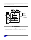
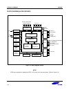

PRODUCT OVERVIEW S3F80JB
1-2
FEATURES
CPU
• SAM8 RC CPU core
Memory
• Program memory:
- 64-Kbyte Internal Flash Memory
- Sector size: 128Bytes
- 10years data retention
- Fast Programming Time: Sector Erase: 10ms
Byte Program: 32us
- Byte Programmable
- User programmable by ‘LDC’ instruction
- Sector (128-bytes) Erase available
- External serial programming support
- Endurance: 10,000 Erase/Program cycles
- Expandable OBPTM (On Board Program)
• Data memory: 272-byte general purpose RAM
Instruction Set
• 78 instructions
• IDLE and STOP instructions added for power-
down modes
Instruction Execution Time
• 500 ns at 8-MHz f
OSC
(minimum)
Interrupts
• 24 interrupt sources with 18 vectors
and 8 levels.
I/O Ports
• Four 8-bit I/O ports (P0–P2 , P4) and 6-bit port
(P3) for a total of 38 bit-programmable pins.
(44-QFP)
• Four 8-bit I/O ports (P0–P2 , P4) and 4-bit port
(P3) for a total of 36 bit-programmable pins.
(42-SDIP)
• Three 8-bit I/O ports (P0–P2) and one 2-bit I/O
port (P3) for a total of 26-bit programmable pins.
(32-SOP)
Carrier Frequency Generator
• One 8-bit counter with auto-reload function and
one-shot or repeat control (Counter A)
Basic Timer and Timer/Counters
• One programmable 8-bit basic timer (BT) for
oscillation stabilization control or watchdog timer
(software reset) function
• One 8-bit timer/counter (Timer 0) with three
operating modes: Interval mode, Capture and
PWM mode.
• One 16-bit timer/counter (Timer1) with two
operating modes: Interval and Capture mode.
• One 16-bit timer/counter (Timer2) with two
operating modes: Interval and Capture mode.
Back-up Mode
• When V
DD
is lower than V
LVD
, the chip enters
Back-up mode to block oscillation and reduce the
current consumption.
In S3F80JB, this function is disabled when
operating state is “STOP mode”.
• When reset pin is lower than Input Low Voltage
(V
IL
), the chip enters Back-up mode to block
oscillation and reduce the current consumption.
Analog Voltage Comparator
• 4-bit resolution: 16-step variable reference
voltage, 150mV Input Voltage Accuracy (worst
case)
• 4-channel mode: CIN0-3, Internal reference
voltage generator
• 3-channel mode: CIN0-2, External reference
voltage source (CIN3) supply
Low Voltage Detect Circuit
• Low voltage detect to get into Back-up mode and
Reset
2.15V (Typ) ± 200mV at 8MHz
1.90V (Typ) ± 200mV at 4MHz
• Low voltage detect to control LVD_Flag bit
2.30V (Typ) ± 200mV at 8MHz
2.15V (Typ) ± 200mV at 4MHz
Operating Temperature Range
• –25
°
C to + 85
°
C
Operating Voltage Range
• 1.95V to 3.6V at 8MHz
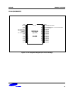
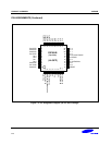
Package Types
• 32-pin SOP
• 44-pin QFP