


BASIC TIMER and TIMER 0 S3F80JB
10-6
TIMER 0 FUNCTION DESCRIPTION
Timer 0 Interrupts (IRQ0, Vectors FAH and FCH)
The timer 0 module can generate two interrupts: the timer 0 overflow interrupt (T0OVF), and the timer 0 match/
capture interrupt (T0INT). T0OVF is interrupt with level IRQ0 and vector FAH. T0INT also belongs to interrupt
level IRQ0, but is assigned the separate vector address, FCH.
A timer 0 overflow interrupt (T0OVF) pending condition is automatically cleared by hardware when it has been
serviced. The T0INT pending condition must, however, be cleared by the application’s interrupt service routine by
writing a “1” to the T0CON.0 interrupt pending bit.
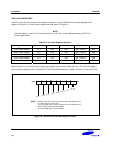
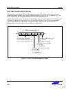
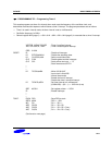
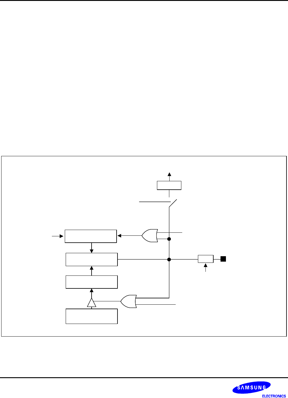
Interval Timer Mode
In interval timer mode, a match signal is generated when the counter value is identical to the value written to the
T0 reference data register, T0DATA. The match signal generates a timer 0 match interrupt (T0INT, vector FCH)
and clears the counter.
If, for example, you write the value ‘10H’ to T0DATA, ‘0BH’ to T0CON, the counter will increment until it reaches
‘10H’. At this point, the T0 interrupt request is generated. And after the counter value is reset, counting resumes.
With each match, the level of the signal at the timer 0 output pin is inverted (See Figure 10-4).
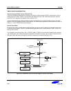
Interrupt
Enable/Disable
(T0CON.1)
CTL
T0CON.5
T0CON.4
T0CON.3
IRQ0(T0INT)
CLK
Match
Pending
(T0CON.0)
Match Signal
P3.0/T0CAP
R (Clear)
T0CON.3
8-Bit Counter
(T0CNT)
8-Bit Comparator
Buffer Register
Timer0 Data Register
(T0DATA)
Figure 10-4. Simplified Timer 0 Function Diagram: Interval Timer Mode