S3F80JB ADDRESS SPACES
2-8
REGISTER SET 1
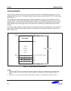
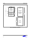
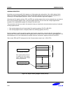
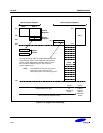
The term set 1 refers to the upper 64 bytes of the register file, locations C0H–FFH.
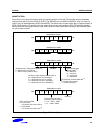
The upper 32-byte area of this 64-byte space (E0H–FFH) is divided into two 32-byte register banks, bank 0 and
bank 1. The set register bank instructions SB0 or SB1 are used to address one bank or the other. In the S3F80JB
microcontroller, bank 1 is implemented. The set register bank instructions, SB0 or SB1, are used to address one
bank or the other. A hardware reset operation always selects bank 0 addressing.
The upper two 32-byte area of set 1, bank 0, (E0H–FFH) contains 31mapped system and peripheral control
registers. Also, the upper 32-byte area of set1, bank1 (E0H–FFH) contains 16 mapped peripheral control register.
The lower 32-byte area contains 15 system registers (D0H–DFH) and a 16-byte common working register area
(C0H–CFH). You can use the common working register area as a “scratch” area for data operations being
performed in other areas of the register file.
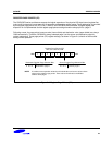
Registers in set 1 locations are directly accessible at all times using the Register addressing mode. The 16-byte
working register area can only be accessed using working register addressing. (For more information about
working register addressing, please refer to Chapter 3, “Addressing Modes,”)
REGISTER SET 2
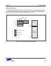
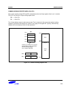
The same 64-byte physical space that is used for set 1 locations C0H–FFH is logically duplicated to add another
64 bytes of register space. This expanded area of the register file is called set 2. The set 2 locations (C0H–FFH)
is accessible on page 0 in the S3F80JB register space.
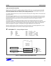
The logical division of set 1 and set 2 is maintained by means of addressing mode restrictions: You can use only
Register addressing mode to access set 1 locations; to access registers in set 2, you must use Register Indirect
addressing mode or Indexed addressing mode.
The set 2 register area is commonly used for stack operations.


