


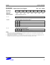

S3F80JB CONTROL REGISTERS
4-3
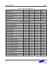
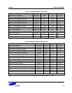
Table 4-1. Mapped Registers (Continued)
Register Name Mnemonic Decimal Hex R/W
Counter A Control Register CACON 243 F3H R/W
Counter A Data Register (High Byte) CADATAH 244 F4H R/W
Counter A Data Register (Low Byte) CADATAL 245 F5H R/W
Timer 1 Counter Register (High Byte) T1CNTH 246 F6H
R
(NOTE)
Timer 1 Counter Register (Low Byte) T1CNTL 247 F7H
R
(NOTE)
Timer 1 Data Register (High Byte) T1DATAH 248 F8H R/W
Timer 1 Data Register (Low Byte) T1DATAL 249 F9H R/W
Timer 1 Control Register T1CON 250 FAH R/W
STOP Control Register STOPCON 251 FBH W
Location FCH is not mapped.
Basic Timer Counter BTCNT 253 FDH
R
(NOTE)
External Memory Timing Register EMT 254 FEH R/W
Interrupt Priority Register IPR 255 FFH R/W
NOTE: You cannot use a read-only register as a destination for the instructions OR, AND, LD, or LDB.
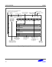
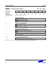
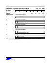
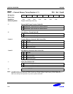
Table 4-2. Mapped Registers (Bank1, Set1)
Register Name Mnemonic Decimal Hex R/W
LVD Control Register LVDCON 224 E0 R/W
Port 3 [4:5] Control Register P345CON 225 E1 R/W
Port 4 Control Register (High Byte) P4CONH 226 E2 R/W
Port 4 Control Register (Low Byte) P4CONL 227 E3 R/W
Timer 2 Counter Register (High Byte) T2CNTH 228 E4
R
(NOTE)
Timer 2 Counter Register (Low Byte) T2CNTL 229 E5
R
(NOTE)
Timer 2 Data Register (High Byte) T2DATAH 230 E6 R/W
Timer 2 Data Register (Low Byte) T2DATAL 231 E7 R/W
Timer 2 Control Register T2CON 232 E8 R/W
Comparator Mode Register CMOD 233 E9 R/W
Comparison Result Register CMPREG 234 EA
R
(NOTE)
Comparator Input Selection Register CMPSEL 235 EB R/W
Flash Memory Sector Address Register (High Byte) FMSECH 236 EC R/W
Flash Memory Sector Address Register (Low Byte) FMSECL 237 ED R/W
Flash Memory User Programming Enable Register FMUSR 238 EE R/W
Flash Memory Control Register FMCON 239 EF R/W
Not mapped in address F0H to 0FFH.
NOTE: You cannot use a read-only register as a destination for the instructions OR, AND, LD, or LDB.