EMBEDDED FLASH MEMORY INTERFACE S3F80JB
15-2
User Program Mode
This mode supports sector erase, byte programming, byte read and one protection mode (Hard Lock Protection).
The S3F80JB has the internal pumping circuit to generate high voltage. Therefore, 12.5V into Vpp (TEST) pin is
not needed. To program a flash memory in this mode several control registers will be used.
There are four kind functions in user program mode – programming, reading, sector erase, and one protection
mode (Hard lock protection).
Tool Program Mode
This mode is for erasing and programming full area of flash memory by external programming tools. The 6 pins of
S3F80JB are connected to a programming tool and then internal flash memory of S3F80JB can be programmed
by Serial OTP/MTP Tools, SPW2 plus single programmer or GW-PRO2 gang programmer and so on. The other
modules except flash memory module are at a reset state. This mode doesn’t support the sector erase but chip
erase (all flash memory erased at a time) and two protection modes (Hard lock protection/ Read protection). The
read protection mode is available only in tool program mode. So in order to make a chip into read protection, you
need to select a read protection option when you write a program code to a chip in tool program mode by using a
programming tool. After read protect, all data of flash memory read “00”. This protection is released by chip erase
execution in the tool program mode.
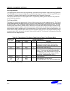
Table 15-1. Descriptions of Pins Used to Read/Write the Flash in Tool Program Mode
During Programming
Normal Chip
Pin Name
Pin Name Pin No. I/O Function
P3.0 SDAT 3[30] I/O Serial data pin. Output port when reading and
input port when writing. SDAT (P3.0) can be
assigned as an input or push-pull output port.
P3.1 SCLK 4[31] I Serial clock pin. Input only pin.
TEST TEST 9[4] I Tool mode selection when TEST pin sets Logic
value ‘1’. If user uses the flash writer tool mode
(ex.spw2+ etc.), user should connect TEST pin to
V
DD
. (S3F80JB supplies high voltage 12.5V by
internal high voltage generation circuit.)
nRESET nRESET 12[7] I Chip Initialization
V
DD
,
V
SS
V
DD
,
V
SS
5[32],
6[1]
– Power supply pin for logic circuit.
V
DD
should be tied to +3.3 V during programming.
NOTE: [ ] means 32SOP package.


