


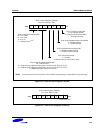
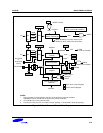

S3F80JB BASIC TIMER and TIMER 0
10-9
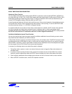
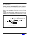
MUX
MUXDIV
R
8-Bit Up-Counter
(T0CNT)
8-Bit Compatator
Timer 0 Buffer
Register
Bits 5, 4
Bit 0
Bit 1
IRQ0
Clear
Data Bus
Bit 0
IRQ0
OVF
8-Bit Up Counter
(BTCNT, Read-Only)
DIV
R
X
IN
X
IN
OVF
RESET
Data Bus
Clear
When BTCNT.4 is set after releasing from
RESET or STOP mode, CPU clock starts.
Match
(2)
Basic Timer Control Register
(Write '1010xxxxB' to disable.)
NOTES:
1. During a power-on reset operation, the CPU is idle during the required oscillation
stabilization interval (until bit 4 of the basic timer counter overflows).
2. It is available only in using internal mode.
3. The external clock source is P3.1/T0CK in 32-pin package, or P3.2/T0CK in 42/44-pin package.
Bits 7, 6
Bits 3, 2
Bit 1
RESET or STOP
(Timer 0 Overflow)
Bit 2
(Timer 0 Match)
T0PWM
Basic Timer Control Register
Timer 0 Control Register
Match Signal
T0CON.3
T0OVF
Data Bus
Timer 0 Data Register
(T0DATA)
1/4096
1/8
1/256
1/4096
1/1024
1/128
P3.0/T0CAP
Bits 5, 4
R
P3.1/T0CK
or
P3.2/T0CK
(note 3)
GND
Bit 3
Figure 10-7. Basic Timer and Timer 0 Block Diagram