


96 Programmer’s Reference Manual
AC ’97 Modem Controller Registers (D30:F3)
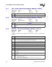
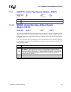
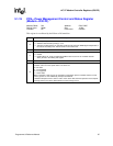
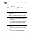
3.1.16 INT_PIN—Interrupt Pin Register (Modem—D30:F3)
Address Offset: 3Dh Attribute: RO
Default Value: See description Size: 8 bits
Lockable: No Power Well: Core
This register indicates which PCI interrupt pin is used for the AC ’97 modem interrupt. The AC ’97
interrupt is internally OR’d to the interrupt controller with the PIRQB# signal.
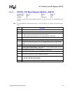
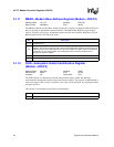
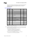
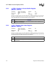
3.1.17 PID—PCI Power Management Capability Identification
Register (Modem—D30:F3)
Address Offset: 50h Attribute: RO
Default Value: 0001h Size: 16 bits
Lockable: No Power Well: Core
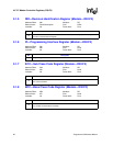
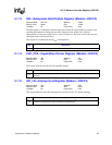
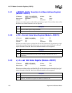
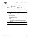
3.1.18 PC—Power Management Capabilities Register
(Modem—D30:F3)
Address Offset: 52h Attribute: RO
Default Value: C9C2h Size: 16 bits
Lockable: No Power Well: Core
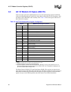
Bit Description
7:3 Reserved
2:0 Interrupt Pin (INT_PN) — RO. This reflects the value of D30IP.AMIP in chipset configuration space.
Bit Description
15:8 Next Capability (NEXT) — RO. This field indicates that this is the last item in the list.
7:0
Capability ID (CAP) — RO. This field indicates that this pointer is a message signaled interrupt
capability.
Bit Description
15:11 PME Support — RO. This field indicates PME# can be generated from all D states.
10:9 Reserved.
8:6
Auxiliary Current — RO. This field reports 375 mA maximum Suspend well current required when in
the D3
COLD
state.
5
Device Specific Initialization (DSI) — RO. This bit indicates that no device-specific initialization is
required.
4 Reserved — RO.
3 PME Clock (PMEC) — RO. This bit indicates that PCI clock is not required to generate PME#.
2:0
Version (VS) — RO. This field indicates support for Revision 1.1 of the PCI Power Management
Specification.