


FX Series Programmable Controlers Applied Instructions 5
5-83
e) The HKY instruction ma
y
onl
y
be used
ONCE
.
f) Normal operation requires 8 scans to read the ke
y
inputs. To achieve a stead
y
and repeatable
performance, constant scan mode should be used,
i.e. M8039 is set ON and a user defined scan time
is written to re
g
ister D8039. However, for a faster
response the HKY instruction should be
pro
g
rammed in a timer interrupt routine as shown
in the example opposite.
Operation 2 - Using the HKY Instruction With
M8167:
(Applicable units: FX
(2C)
and FX
2N
)
When the HKY instruction is used with fla
g
M8167 ON
(as shown ri
g
ht), the operation of ke
y
s A throu
g
h F
allow actual entr
y
of the Hexadecimal values of A
throu
g
h F respectivel
y
into the data device D
2
. This is
in addition to the standard 0 throu
g
h 9 ke
y
s. All other
operation is as specified in ‘Operation 1 - Standard’.
Maximum stora
g
e values for this operation become
FFFF in 16 bit mode and FFFFFFFF in 32 bit (double
word) mode.
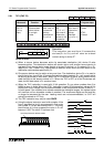
5.8.3 DSW (FNC 72)
Operation:
This instruction multiplexes 4 outputs (D
1
) throu
g
h 1
or 2(n) sets of switches. Each set of switches
consists of 4 thumbwheels providin
g
a sin
g
le di
g
it
input.
Points to note:
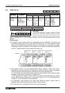
a) When n = 1 onl
y
one set of switches are read. The
multiplex is completed b
y
wirin
g
the thumbwheels
in parallel back to 4 consecutive inputs from the
head address specified in operand S. The (4 di
g
it)
data read is stored in data device D
2
.
Continued on next pa
g
e...
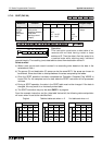
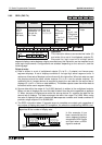
Mnemonic Function
Operands
Program steps
S
D
1
D
2
n
DSW
FNC 72
(Di
g
ital
switch)
Multiplexed
readin
g
of n sets
of di
g
ital (BCD)
thumbwheels
X
Note:
If n=2 then
8
devices
else 4.
Y
Note:
uses 4
consecu-
tive
devices
T, C, D, V, Z
Note: If
n=2 then 2
devices
else 1.
K, H
Note:
n= 1 or 2
DSW:
9 steps
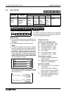
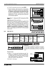
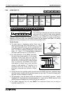
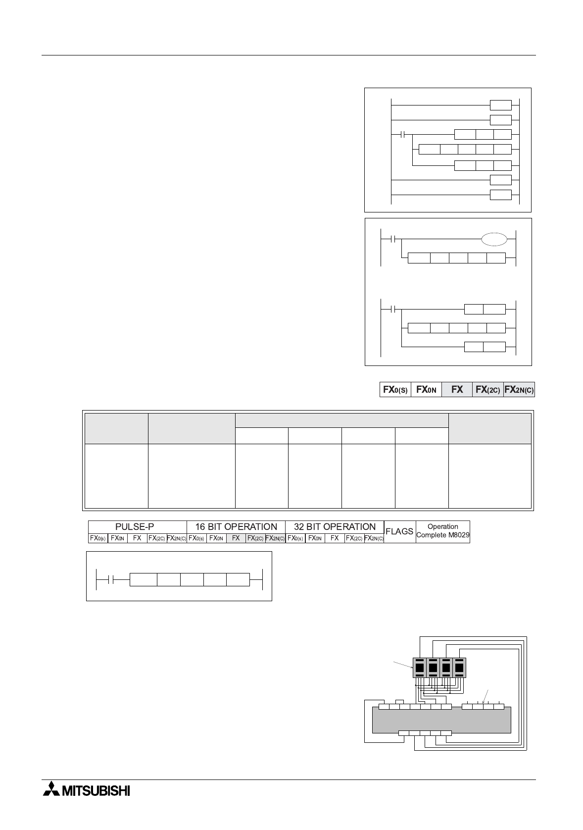
Y 0 D 0 M 0HKY X 0
EI
FEND
K8REF X 0
K8REF Y0
IRET
END
M8000
I 610
X17
Y 60 D 5 M90
HKY
X 10
M8167
X17
Y 60 D 5 M90
HKY
X 10
SET
M8167
RST
M8167
These two program examples
perform the same task.
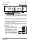
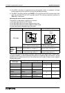
X0
Y 10 D 0
[ D2 ]
K 1DSW
[ D1 ]
X 10
[ S ] [ n ]
1248
4 2 1
10 10 10
012
3
X11 X12 X13
24V
0V S/S
X14 X15 X16 X17
Y12 Y13+V Y10 Y11
1248
X10
3
10
Transistor Outputs (source)
BCD digital
switches
(1st set)
2nd
switch
set inputs