


10
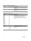
Signal name Pin # Type(I/O) Signal description
MDIO 113 I/O MII management input/output serial data. When this interface
is unused, connect this pin high. If HDMP-3001 is attached
to a MAC via the mechanical interface specified in IEEE 802.3,
clause 22.6, an external pull-up of 1.5 kohm ± 5% is required.
MDC 114 I MII management clock, up to 2.5 MHz. When this interface is
unused, connect this pin high.
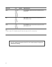
Signal name Pin # Type(I/O) Signal description
RX_E1_DATA 38 O RECEIVED E1 DATA: Local orderwire channel data byte
(E1) received from the line side.
RX_E2_DATA 37 O RECEIVED E2 DATA: Express orderwire channel data byte
(E2) received from the line side.
RX_F1_DATA 36 O RECEIVED F1 DATA: Maintenance channel data byte (F1)
received from the line side.
RX_E1E2F1_CLK 35 O RECEIVED E1/E2/F1 DATA REFERENCE CLOCK: A
64 kHz clock reference output for E1/E2/F1 data. The MSB of
the E1/E2/F1 bytes appears in the first 64 kHz clock cycle
after a rising edge of RX_FRAME_SFP.
RX_FRAME_SFP 158 O RECEIVE FRAMER START-OF-FRAME INDICATION: This signal is
nominally 8 kHz and is high during the first row of overhead
of the received frame. The RX_FRAME_SFP signal is also used
for byte alignment of the received E1/E2/F1 data outputs. This
is a SFP (Start-of-Frame-Pulse) indicating the SONET frame
position on the RX_DATA [7:0] bus.
RX_LDCC_DATA 154 O RECEIVED LINE DCC DATA: Drop output for received
Line Data Communications Channel (DCC).
RX_LDCC_CLK 155 O RECEIVED LINE DCC REFERENCE CLOCK : A gapped 576 kHz clock
reference for Line DCC data. The RX_LDCC_DATA outputs are
updated on the falling edge of RX_LDCC_CLK.
RX_SDCC_DATA 156 O RECEIVED SECTION DCC DATA: Drop output for received Section
Data Communications Channel (DCC).
RX_8K_CLK 146 O 8kHz RECEIVE CLOCK: A general purpose 8kHz buffered clock
derived from RX_SONETCLK which may be used for external
clock reference purposes.
RX_SDCC_CLK 157 O RECEIVED SECTION DCC REFERENCE CLOCK : A gapped 192 kHz
clock reference for Section DCC data. The RX_SDCC_DATA out-
puts are updated on the falling edge of RX_SDCC_CLK.
Table 3. Transport Overhead Pins Description
(continues)