


40
4.3 Firmware and System Design
Information
4.3.1 Board level pull-ups and
pull-downs
Many of the HDMP-3001 input and
tristateable outputs have internal
pull-ups. Refer to the pin descrip-
tion for detailed information on
where external pull-ups are re-
quired.
4.3.2 Motorola MPC860
Microprocessor Interface
The recommended setup of the
interface is:
• HDMP-3001 mapped to the
smallest memory bank, 32
Kbytes.
• BR[20-31] = 010000000001,
which sets no parity, 8 bits
data, GPCM controlled.
• OR[20-31] = 000100001000,
which sets normal CS timing,
no burst allowed, externally
generated TA.
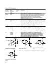
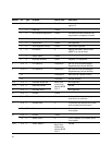
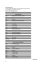
Pin connections are described in
Table 16.
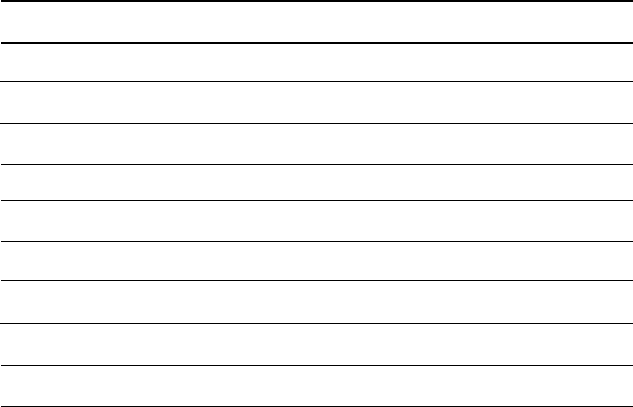
HDMP-3001 Pin Name Microprocessor Pin Name
HDMP-3001 Pin Name Microprocessor Pin Name
BUSMODE [1:0] 0, 0
ADDR[8] to ADDR[0] A[23] to A[31]. Note: Bus is twisted!
D[7] to D[0] D[0] to D[7]. Note: Bus is twisted!
CSB One of the CSs
WRB WE0
RDB OE
RDYB TA
INTB One of the IRQs
CPU_CLK CLKOUT
Table 16. Pin Connections – MPC860