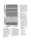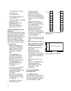
28
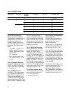
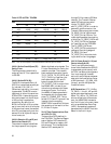
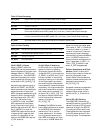
Row Column
1 2-3 4 5-6 7 8-9
1 A1[1] A1[2,3] A2[1] A2[2,3] J0[1] Z0[2,3]
2B1 E1 F1
3D1 D2 D3
4 H1[1] H1[2,3] H2[1] H2[2,3] H3[1] H3[2,3]
5 B2[1] B2[2,3] K1 K2
6D4 D5 D6
7D7 D8 D9
8 D10 D11 D12
9 S1 Z1[2,3]
1
Z2[1]
1
Z2[2]
1
, M1 E2
Table 12. STS-3c/STM-1 TOH/SOH
3.9.3.3.4 Section Growth/Spare (ZO)
Section Trace
The Z0 bytes are transmitted in
order as 2 and 3. This is specified
in GR-253.
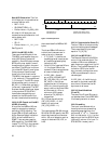
3.9.3.3.5 Section BIP-8 (B1)
The B1 Bit Interleaved Parity 8
(BIP-8) is transmitted as even par-
ity (normal) if B1_INV = 0.
Otherwise, odd parity (incorrect)
is generated. The BIP-8 is calcu-
lated over all bits of the previous
STS-3c/STM-1 frame after scram-
bling and placed into the B1 byte
of the current frame before
scrambling. By definition of
BIP-8, the first bit of B1 provides
parity over the first bit of all bytes
of the previous frame, the second
bit of B1 provides parity over the
second bit of all bytes of the pre-
vious frame, etc.
3.9.3.3.6 Orderwire (E1 and E2) and
Section User Channel (F1)
The orderwire bytes are defined
for the purpose of carrying two
64kb/s digitized voice signals. The
F1 byte is available for use by the
network provider. The transmit
block accepts three serial inputs,
TX_E1_DATA, TX_E2_DATA, and
TX_F1_DATA, for insertion into
the transmitted E1, E2, and F1
bytes. A single 64 kHz clock
(TX_E1E2F1_CLK) is output from
the HDMP-3001 in order to pro-
vide a timing reference for these
three serial inputs. The first bit
(the MSB) of these bytes should
correspond with the frame start
pulse, TX_FRAME_SFP. The re-
ceived E1, E2 and F1 bytes will be
inserted into the outgoing
SONET/SDH frame which follows
the reception of the last bit of the
E1, E2 and F1 bytes.
3.9.3.3.7 Data Communications Chan-
nels, DCC, (D1-D12)
There are two DCCs defined in
the TOH/SOH. The Section/Regen-
erator Section DCC uses the D1,
D2, and D3 bytes to create a 192
kb/s channel. The Line/Multiplex
Section DCC uses bytes D4
through D12 to create a 576 kb/s
channel. The Transmit Side ac-
cepts DCC data on two serial
inputs, TX_SDCC_DATA
and TX_LDCC_DATA. In order to
assure bit synchronization, the
Transmit Side outputs two clocks,
TX_SDCC_CLK at 192 kHz and
TX_LDCC_CLK at 576 kHz. The
clock signals enable the clocking
of bits from TX_SDCC_DATA and
TX_LDCC_DATA into registers
for inserting into the TOH/SOH.
The TX_SDCC_DATA and
TX_LDCC_DATA inputs should
change on the falling edges of
TX_SDCC_CLK and
TX_LDCC_CLK, since the clock-
ing is done on the rising edges.
3.9.3.3.8 Pointer Bytes (H1, H2) and
Pointer Action Byte (H3)
The H1 and H2 bytes contain
three fields. Because the SPE/VC
is generated synchronously with
the TOH, variable pointer genera-
tion is not required. Instead,
active H1 and H2 bytes are gener-
ated with the fixed pointer value
of 522 (decimal) = 10_0000_1010
(binary), and the H3 bytes are
fixed at all zeros.
AIS Generation: If TX_LAIS or
TX_PAIS = 1, the H1, H2, and H3
bytes are transmitted as all ones.
When TX_LAIS or TX_PAIS tran-
sitions so that both bits become
zero, the HDMP-3001 transmits
the first H1 byte in the next frame
with an enabled New Data Flag
(NDF). Succeeding frames are
generated with the NDF field dis-
abled in the first H1 byte.
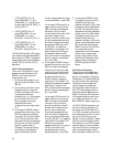
Note: 1. The Z1 and Z2 bytes are nonstandardized reserved bytes for STM-1.


