


2
3.9 SONET/SDH Processing................................................................. 24
3.9.1 Transmit SONET/SDH Processing Overview ...................... 24
3.9.2 Receive SONET/SDH Processing Overview ........................ 25
3.9.3 Transmit SONET/SDH Processing Details ........................... 25
3.9.4 Receive SONET/SDH Processing Details ............................. 30
4. Application Information ........................................................................ 38
4.1 Chip setup and configuration ........................................................ 38
4.1.1 EEPROM Detection ................................................................. 38
4.2 Configurations ................................................................................. 38
4.2.1 PHY and MAC mode ................................................................ 38
4.2.2 SDH and SONET mode ........................................................... 38
4.2.3 LAPS and GFP mode ............................................................... 38
4.2.4 INT Pin Configuration ............................................................. 38
4.3 Firmware and System Design Information ................................. 40
4.3.1 Board level pull-ups and pull-downs.................................... 40
4.3.2 Motorola MPC860 Microprocessor Interface ...................... 40
4.3.3 MII Interface ............................................................................. 41
4.3.4 EEPROM Interface .................................................................. 41
5. Register Definitions ............................................................................... 42
5.1 MII Management Register Map .................................................... 42
5.2 Chip Register Map ........................................................................... 44
5.3 SONET/SDH Transmit Registers................................................... 56
5.4 SONET/SDH Receive Registers..................................................... 61
5.5 Ethernet Transmit Registers ......................................................... 79
5.6 Ethernet Receive Registers ........................................................... 88
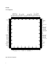
6. Package Specification .......................................................................... 104
7. Electrical and Thermal Specifications............................................... 107
7.1 Technology..................................................................................... 107
7.2 Maximum Ratings ......................................................................... 107
7.3 Thermal Characteristics ............................................................... 107
7.4 DC Characteristics ........................................................................ 108
7.5 AC Electrical Characteristics ...................................................... 108
7.5.1 General AC Specifications.................................................... 108
7.5.2 MII Specifications .................................................................. 109
8. Timing Diagrams .................................................................................. 110
8.1 Microprocessor Bus Timing - Write Cycle................................. 110
8.2 Microprocessor Bus Timing - Read Cycle ................................. 111
8.3 Microprocessor Bus Timing Table. ............................................ 112
8.4 Line Interface Receive and Transmit Timing ............................ 112
8.5 TOH Interface E1/E2/F1 Transmit Timing................................. 113
8.6 TOH Interface E1/E2/F1 Receive Timing................................... 114
8.7 DCC Interface Transmit Timing .................................................. 114
8.8 DCC Interface Receive Timing .................................................... 115
8.9 JTAG Interface Timing ................................................................. 115
8.10 Reset specification..................................................................... 116
8.11 MII Timing ................................................................................... 116
8.12 MDIO Port Timing ...................................................................... 117
8.13 EEPROM Port Timing ................................................................ 118
8.14 In Frame Declaration................................................................. 118
9. Applicable Documents ......................................................................... 124