66
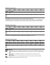
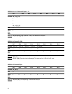
Bit 7 Bit 6 Bit 5 Bit 4 Bit 3 Bit 2 Bit 1 Bit 0
Bit name RX_J0 [0]_[7:0]
•
•
•
RX_J0 [15]_[7:0]
R/W R
Value 0
after
reset
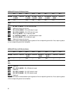
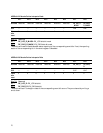
ADDR=0x104 –0x113: Receive J0 Bytes 0 – 15
Bits 7-0: RX_J0 [0:15]_[7:0]: (Section Trace) The received 16 J0 bytes.
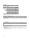
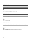
Bit 7 Bit 6 Bit 5 Bit 4 Bit 3 Bit 2 Bit 1 Bit 0
Bit name Reserved Reserved Reserved Reserved RX_S1[3:0]
R/W ———— R
Value 0000 0 0 0 0
after
reset
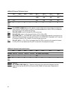
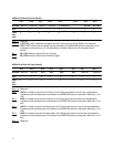
ADDR=0x114: Receive S1 LSBs
Bits 7-4: Reserved
Bits 3-0: RX_S1 [3:0]: (Synchronization Message) The received four LSBs of the S1 byte.
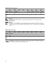
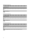
Bit 7 Bit 6 Bit 5 Bit 4 Bit 3 Bit 2 Bit 1 Bit 0
Bit name RX_K2[7:0]
R/W R
Value 0000 0 0 0 0
after
reset
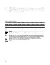
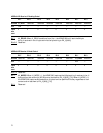
ADDR=0x115: Receive K2 Byte
Bits 7-0: RX_K2 [7:0]: (APS Signaling) The received K2 byte.


