


3
List of Figures
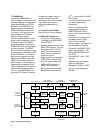
Figure 1. Functional Block Diagram ......................................................... 5
Figure 2. HDMP-3001 applications ............................................................ 6
Figure 3. HDMP-3001 pin assignments ..................................................... 7
Figure 4. GFP Payload Bit Order ............................................................. 18
Figure 5. GFP FCS Bit Order .................................................................... 18
Figure 6. LAPS Payload Bit Order ........................................................... 19
Figure 7. LAPS FCS Bit Order .................................................................. 19
Figure 8. Loopbacks .................................................................................. 20
Figure 9. An Ethernet MAC frame ........................................................... 22
Figure 10. The format of a LAPS frame with a MAC payload.............. 22
Figure 11. The GFP frame......................................................................... 24
Figure 12. The structure of the SONET STS-3c SPE and SDH VC-4 ...25
Figure 13. STS-3c SPE or VC-4 Structure ............................................... 25
Figure 14. Pointer Byte Fields.................................................................. 29
Figure 15. Pointer Processing .................................................................. 33
Figure 16. Pointer tracking algorithm. .................................................... 33
Figure 17. Functional block of SONET framer scrambler ................... 36
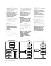
Figure 18. HDMP-3001 connecting to a MAC ......................................... 38
Figure 19. HDMP-3001 connecting to a PHY.......................................... 38
Figure 20. Mode = 00, O/D (Default) ...................................................... 39
Figure 21. Mode = 01, O/S ......................................................................... 39
Figure 22. Mode = 10, Always Enabled, Active-0 .................................. 39
Figure 23. Mode = 11, Always Enabled, Active-1 .................................. 39
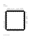
Figure 24. Package Marking ................................................................... 104
Figure 25. Top View of Package ............................................................ 104
Figure 26. Bottom View of Package ...................................................... 105
Figure 27. Side View of Package ........................................................... 105
Figure 28. Detailed View of Pin ............................................................. 105
Figure 29. Microprocessor Write Cycle Timing ................................... 110
Figure 30. Microprocessor Read Cycle Timing ................................... 111
Figure 31. Line Interface Transmit Timing........................................... 112
Figure 32. Line Interface Receive Timing............................................. 113
Figure 33. TOH Interface E1/E2/F1 Transmit Timing. ........................ 113
Figure 34. TOH Interface E1/E2/F1 Receive Timing ........................... 114
Figure 35. DCC Interface Transmit Timing .......................................... 114
Figure 36. DCC Interface Receive Timing ............................................ 115
Figure 37. JTAG Interface Timing ......................................................... 115
Figure 38. MII timing as defined by IEEE 802.3 .................................. 116
Figure 39. In Frame Declaration. ........................................................... 118
Figure 40. Out of Frame Declaration ................................................... 119
Figure 41. Loss of Frame Declaration/Removal .................................. 119
Figure 42. Line AIS and Line RDI Declaration/Removal .................... 119
Figure 43. Transmit Overhead Clock and Data Alignment ................ 120
Figure 44. Receive Overhead Clock and Data Alignment .................. 121
Figure 45. Transmit Data Link Clock and Data Alignment ................ 122
Figure 46. Receive Data Link Clock and Data Alignment .................. 123