


112
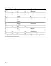
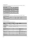
8.3 Microprocessor Bus Timing Table
Table 30. Timing of microprocessor bus
Parameter Description Min (ns) Max (ns)
t
1
CS_N active to RDYB driven to inactive state 0 15
t
2
CS_N, WRB and RDB valid to A and D captured 90 270
t
3
1
CS_N, WRB and RDB valid to RDYB active 140
1
220
1
t
4
BUSMODE 0: WRB inactive to RDYB inactive 0 15
BUSMODE 1: RDB inactive to RDYB inactive
t
5
CS_N inactive to RDYB in high impedance state 0 15
t
6
CS_N, WRB and RDB valid to GPIO outputs updated (when the 250 370
GPIOs are the target of the write cycle)
t
7
CS_N, WRB and RDB valid to A captured 90 270
t
8
CS_N, WRB and RDB valid to GPIO inputs captured (when the 300 520
GPIOs are the target of the read cycle)
t
9
CS_N, WRB and RDB valid to D valid 600 750
t
10
1
D valid to RDYB active 50
1
60
1
t
11
CS_N, WRB and RDB valid to RDYB active 650 850
t
12
RDB inactive to D in high impedance state 0 15
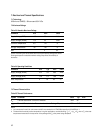
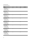
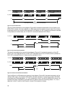
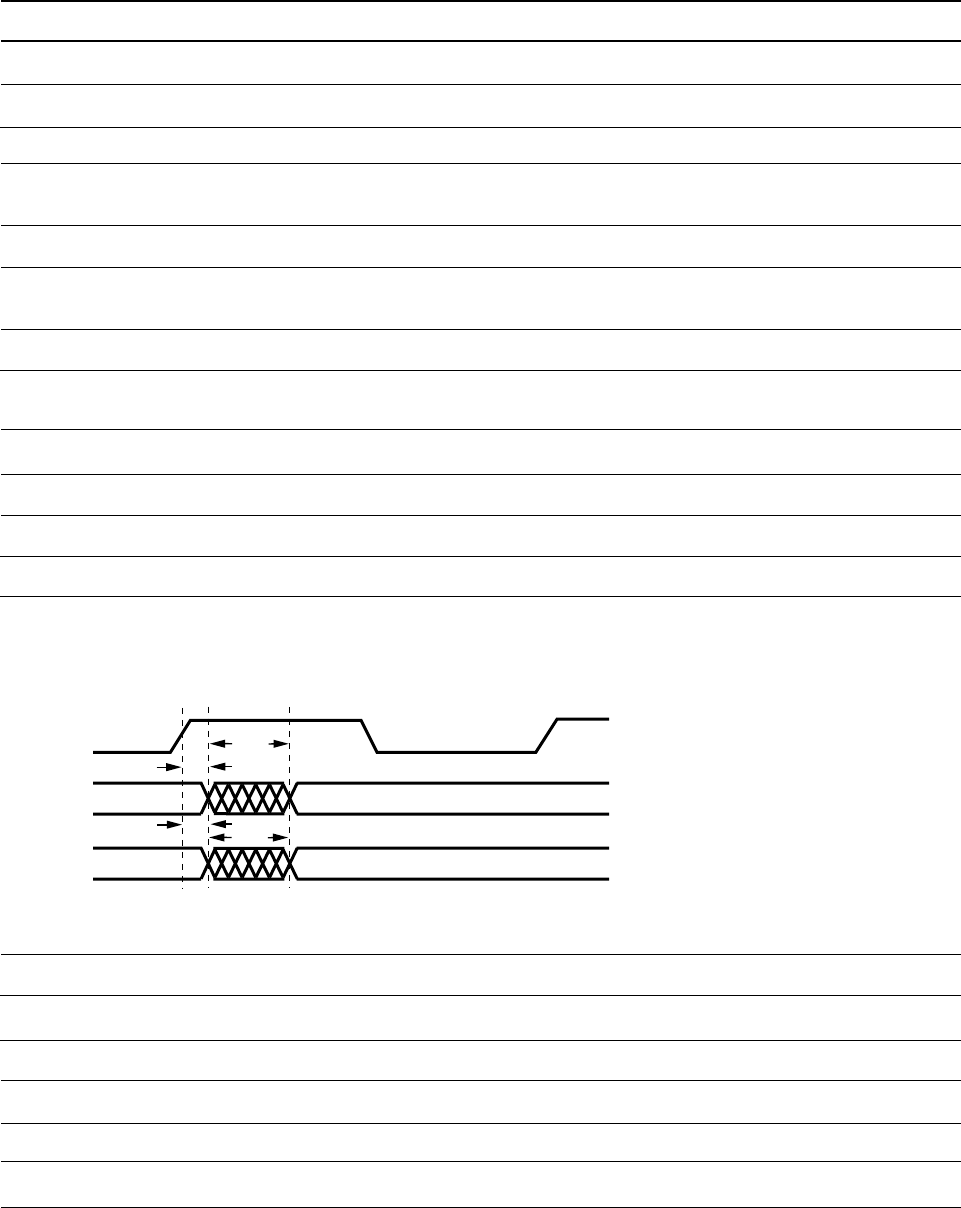
8.4 Line Interface Receive and Transmit Timing
Label Parameter Min Max Units
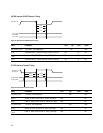
TX_SONETCLK TX_SONETCLK frequency 19.44-20ppm 19.44+20ppm MHz
t
HTDFC
TX_DATA hold time 1 ns
t
VTDFC
TX_DATA transition from TX_CLK high 15 ns
t
HFOFC
TX_FRAME_SFP hold time 1 ns
t
VFOFC
TX_FRAME_SFP transition from TX_CLK high 15 ns
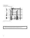
Figure 31. Line Interface Transmit Timing
Note 1: RDYB is re-clocked twice by the microprocessor clock in addition to the timing shown. This adds an additional delay of
between one and two microprocessor clock cycles.
TX_SONETCLK
TX_DATA[7:0]
TX_FRAME_SFP
t
HTDFC
t
HFOFC
t
VFOFC
t
VTDFC