


Rev. 1.0, 07/01, page 86 of 372
7.3 On-Board Programming Modes
There are two modes for programming/erasing of the flash memory; boot mode, which enables on-
board programming/erasing, and programmer mode, in which programming/erasing is performed
with a PROM programmer. On-board programming/erasing can also be performed in user
program mode. At reset-start in reset mode, this LSI changes to a mode depending on the TEST
pin settings, NMI pin settings, and input level of each port, as shown in table 7-1. The input level
of each pin must be defined four states before the reset ends.
When changing to boot mode, the boot program built into this LSI is initiated. The boot program
transfers the programming control program from the externally-connected host to on-chip RAM
via SCI3. After erasing the entire flash memory, the programming control program is executed.
This can be used for programming initial values in the on-board state or for a forcible return when
programming/erasing can no longer be done in user program mode. In user program mode,
individual blocks can be erased and programmed by branching to the user program/erase control
program prepared by the user.
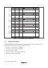
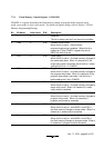
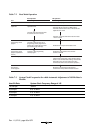
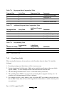
Table 7-1 Setting Programming Modes
TEST NMI P85 PB0 PB1 PB2 LSI State after Reset End
01XXXXUser Mode
001XXXBoot Mode
1 X X 0 0 0 Programmer Mode
Legend:X:Don’t care.
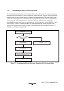
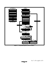
7.3.1 Boot Mode
Table 7-2 shows the boot mode operations between reset end and branching to the programming
control program.
1. When boot mode is used, the flash memory programming control program must be prepared in
the host beforehand. Prepare a programming control program in accordance with the
description in section 7.5, Flash Memory Programming/Erasing.
2. SCI3 should be set to asynchronous mode, and the transfer format as follows: 8-bit data, 1 stop
bit, and no parity.
3. When the boot program is initiated, the chip measures the low-level period of asynchronous
SCI communication data (H'00) transmitted continuously from the host. The chip then
calculates the bit rate of transmission from the host, and adjusts the SCI3 bit rate to match that
of the host. The reset should end with the RxD pin high. The RxD and TxD pins should be
pulled up on the board if necessary. After the reset is complete, it takes approximately 100
states before the chip is ready to measure the low-level period.