


Rev. 1.0, 07/01, page 92 of 372
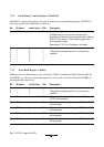
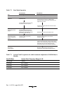
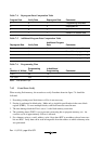
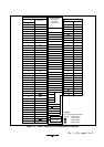
Table 7-4 Reprogram Data Computation Table
Program Data Verify Data Reprogram Data Comments
0 0 1 Programming completed
0 1 0 Reprogram bit
101 —
1 1 1 Remains in erased state
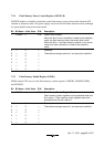
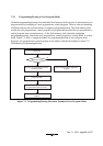
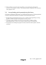
Table 7-5 Additional-Program Data Computation Table
Reprogram Data Verify Data
Additional-Program
Data Comments
0 0 0 Additional-program bit
0 1 1 No additional programming
1 0 1 No additional programming
1 1 1 No additional programming
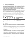
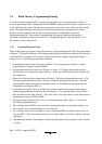
Table 7-6 Programming Time
n
(Number of Writes)
Programming
Time
In Additional
Programming Comments
1 to 6 30 10
7 to 1,000 200 —
Note: Time shown in µs.
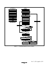
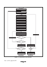
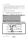
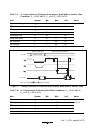
7.4.2 Erase/Erase-Verify
When erasing flash memory, the erase/erase-verify flowchart shown in figure 7-4 should be
followed.
1. Prewriting (setting erase block data to all 0s) is not necessary.
2. Erasing is performed in block units. Make only a single-bit specification in the erase block
register (EBR1). To erase multiple blocks, each block must be erased in turn.
3. The time during which the E bit is set to 1 is the flash memory erase time.
4. The watchdog timer (WDT) is set to prevent overerasing due to program runaway, etc. An
overflow cycle of approximately 19.8 ms is allowed.
5. For a dummy write to a verify address, write 1-byte data H'FF to an address whose lower two
bits are B'00. Verify data can be read in longwords from the address to which a dummy write
was performed.