


Rev. 1.0, 07/01, page 70 of 372
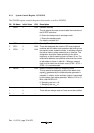
6.1.1 System Control Register 1(SYSCR1)
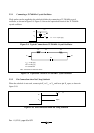
The SYSCR1 register controls the power-down modes, as well as SYSCR2.
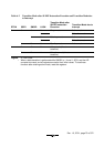
Bit Bit Name Initial Value R/W Description
7 SSBY 0 R/W Software Standby
This bit selects the mode to transit after the execution of
the SLEEP instruction.
0: Enters the sleep mode or subsleep mode.
1: Enters the standby mode.
For details, see table 6-2.
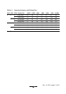
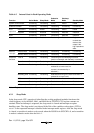
6
5
4
STS2
STS1
STS0
0
0
0
R/W
R/W
R/W
Standby Timer Select 2 to 0
These bits designate the time the CPU and peripheral
modules wait for stable clock operation after exiting from
the standby mode, subactive mode, or subsleep mode to
the active mode or sleep mode due to an interrupt. The
designation should be made according to the clock
frequency so that the waiting time is at least 10 ms.
The
relationship between the specified value and the number
of wait states is shown in table 6-1. When an external
clock is to be used, the minimum value (STS2 = STS1 =
STS0 =1) is recommended.
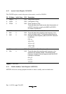
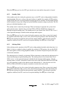
3 NESEL 0 R/W Noise Elimination Sampling Frequency Select
This bit selects the frequency at which the watch clock
signal(φ
W
)generated by the subclock pulse generator is
sampled, in relation to the oscillator clock(φ
OSC
)generated
by the system clock pulse generator. When φ
OSC
=2 to 10
MHz, clear NESEL to 0.
0: Sampling rate is φ
OSC
/16
1: Sampling rate is φ
OSC
/4
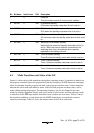
2
1
0
−
−
−
0
0
0
−
−
−
Reserved
These bits are always read as 0 and cannot be modified.