


Rev. 1.0, 07/01, page 244 of 372
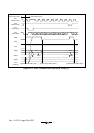
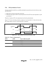
12 781 78 1
SCL
TRS
Bit 0
Data 1
Data 1
Data 2 Data 3
Data 2 Data 3
Bit 6 Bit 7 Bit 0 Bit 6 Bit 7 Bit 0
Bit 1
SDA
(Output)
TDRE
ICDRT
ICDRS
User
processing
[3] Write data
to ICDRT
[3] Write data
to ICDRT
[3] Write data
to ICDRT
[3] Write data
to ICDRT
[2] Set TRS
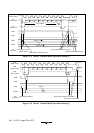
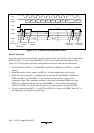
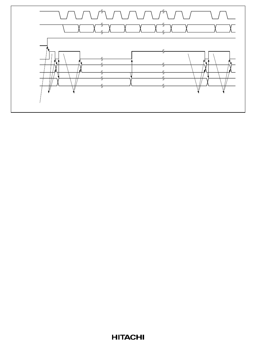
Figure 15-14 Transmit Mode Operation Timing
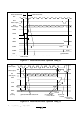
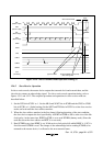
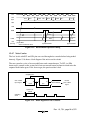
Receive Operation
In receive mode, data is latched at the rise of the transfer clock. The transfer clock is output when
MST in ICCR1 is 1, and is input when MST is 0. For receive mode operation timing, refer to
figure 15-15. The reception procedure and operations in receive mode are described below.
1. Set the ICE bit in ICCR1 to 1. Set the MST and CKS3 to CKS0 bits in ICCR1 to 1. (Initial
setting)
2. When the transfer clock is output, set MST to 1 to start outputting the receive clock.
3. When the receive operation is completed, data is transferred from ICDRS to ICDRR and
RDRF in ICSR is set. When MST = 1, the next byte can be received, so the clock is
continually output. The continuous reception is performed by reading ICDRR every time
RDRF is set. When the 8th clock is risen while RDRF is 1, the overrun is detected and
AL/OVE in ICSR is set. At this time, the previous reception data is retained in ICDRR.
4. To stop receiving when MST = 1, set RCVD in ICCR1 to 1, then read ICDRR. Then, SCL is
fixed high after receiving the next byte data.