


Rev. 1.0, 07/01, page 132 of 372
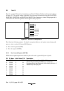
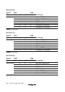
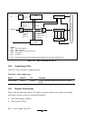
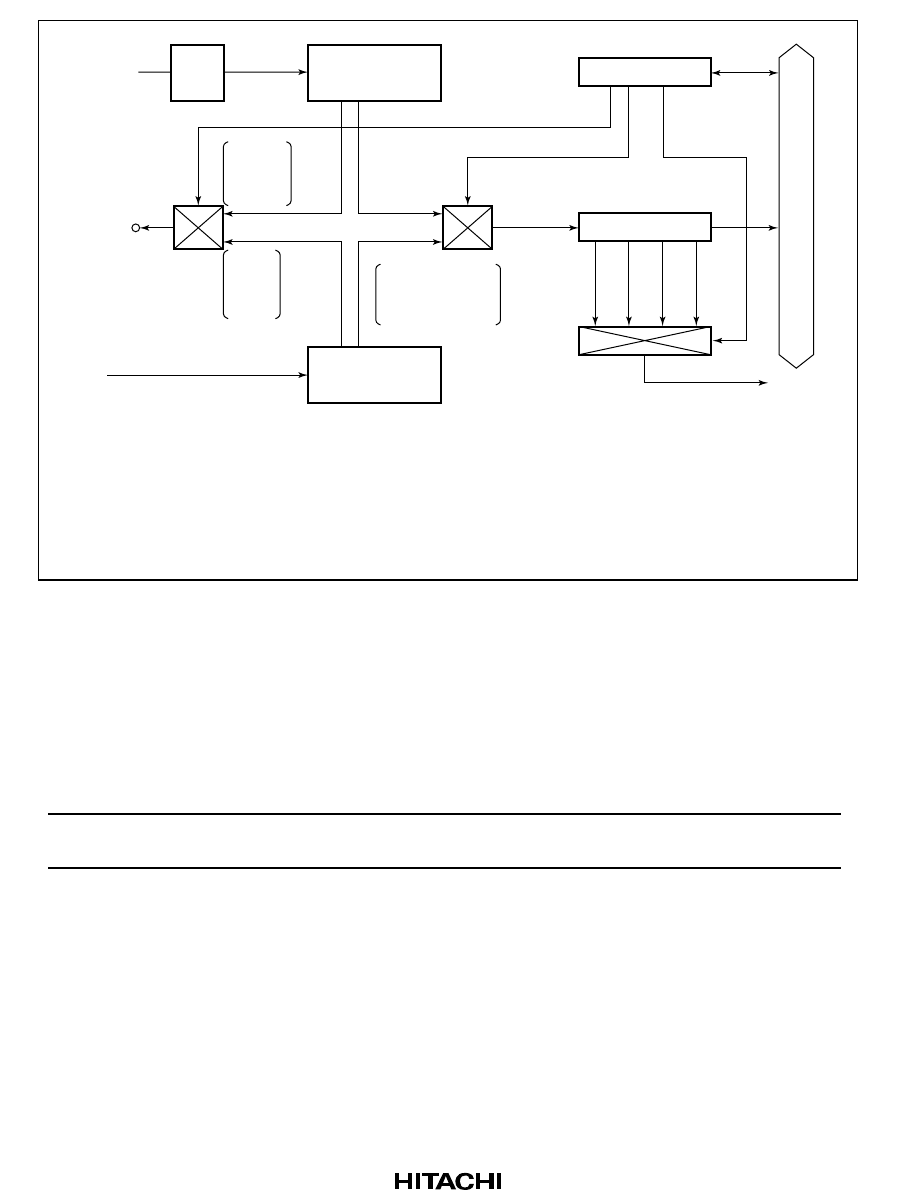
ø
W
TMOW
ø
ø
W
/32
ø
W
/16
ø
W
/8
ø
W
/4
ø
W
/32
ø
W
/16
ø
W
/8
ø
W
/4
ø/8192, ø/4096,
ø/2048, ø/512,
ø/256, ø/128,
ø/32, ø/8
ø
W
/128
ø
W
/4
1/4
PSW
PSS
TMA
TCA
IRRTA
÷8*
÷64*
÷128*
÷256*
Legend
TMA: Timer mode register A
TCA: Timer counter A
IRRTA: Timer A overflow interrupt request flag
PSW: Prescaler W
PSS: Prescaler S
Note: * Can be selected only when the prescaler W output (ø
W
/128) is used as the TCA input clock.
Internal data bus
Figure 10-1 Block Diagram of Timer A
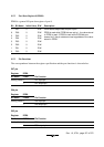
10.2 Input/Output Pins
Table 10-1 shows the timer A input/output pin.
Table 10-1 Pin Configuration
Name Abbrev. I/O Function
Clock output TMOW Output Output of waveform generated by timer A output
circuit
10.3
Register Descriptions
Timer A has the following registers. For details on register addresses and register states during
each process, refer to section 19, Internal I/O Registers.
•
Timer mode register A(TMA)
•
Timer counter A(TCA)