


Rev. 1.0, 07/01, page 84 of 372
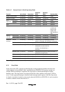
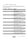
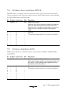
7.2.2 Flash Memory Control Register 2 (FLMCR2)
FLMCR2 is a register that displays the state of flash memory programming/erasing. FLMCR2 is a
read-only register, and should not be written to.
Bit Bit Name Initial Value R/W Description
7 FLER 0 R Flash Memory Error
Indicates that an error has occurred during an
operation on flash memory (programming or erasing).
When FLER is set to 1, flash memory goes to the
error-protection state.
See section 7.5.3, Error Protection, for details.
6
5
4
3
2
1
0
—
—
—
—
—
—
—
0
0
0
0
0
0
0
—
—
—
—
—
—
—
Reserved
These bits are always read as 0, and cannot be
modified.
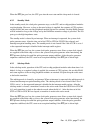
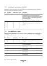
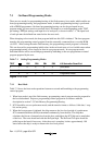
7.2.3 Erase Block Register 1 (EBR1)
EBR1 specifies the flash memory erase area block. EBR1 is initialized to H'00 when the SWE bit
in FLMCR1 is 0. Do not set more than one bit at a time, as this will cause all the bits in EBR1 to
be automatically cleared to 0.
Bit Bit Name Initial Value R/W Description
7
6
5
—
—
—
0
0
0
—
—
—
Reserved
These bits are always read as 0, and cannot be
modified.
4 EB4 0 R/W When this bit is set to 1, 28 kbytes of H'1000 to
H'7FFF will be erased.
3 EB3 0 R/W When this bit is set to 1, 1 kbyte of H'0C00 to H'0FFF
will be erased.
2 EB2 0 R/W When this bit is set to 1, 1 kbyte of H'0800 to H'0BFF
will be erased.
1 EB1 0 R/W When this bit is set to 1, 1 kbyte of H'0400 to H'07FF
will be erased.
0 EB0 0 R/W When this bit is set to 1, 1 kbyte of H'0000 to H'03FF
will be erased.