


Rev. 1.0, 07/01, page 261 of 372
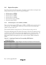
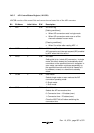
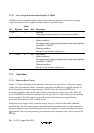
Table 16-3 A/D Conversion Time (Single Mode)
CKS = 0 CKS = 1
Item Symbol Min Typ Max Min Typ Max
A/D conversion start delay time t
D
6—9 4—5
Input sampling time t
SPL
—31— —15—
A/D conversion time t
CONV
131 — 134 69 — 70
Note: All values represent the number of states.
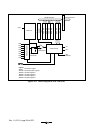
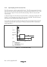
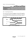
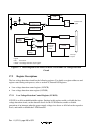
16.4.4 External Trigger Input Timing
A/D conversion can also be started by an external trigger input. When the TRGE bit in ADCR is
set to 1, external trigger input is enabled at the ADTRG pin. A falling edge at the ADTRG input
pin sets the ADST bit in ADCSR to 1, starting A/D conversion. Other operations, in both single
and scan modes, are the same as when the bit ADST has been set to 1 by software. Figure 16-3
shows the timing.
ø
Internal trigger signal
ADST
A/D conversion
Figure 16-3 External Trigger Input Timing