


Rev. 1.0, 07/01, page 166 of 372
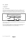
12.4.2 PWM Operation
In PWM mode, PWM waveforms are generated by using GRA as the period register and GRB,
GRC, and GRD as duty registers. PWM waveforms are output from the FTIOB, FTIOC, and
FTIOD pins. Up to three-phase PWM waveforms can be output. In PWM mode, a general register
functions as an output compare register automatically. The output level of each pin depends on the
corresponding timer output level set bit(TOB, TOC, TOD) in TCRW. When TOB is 1, the FTIOB
output goes to 1 at compare match A and to 0 at compare match B. When TOB is 0, the FTIOB
output goes to 0 at compare match A and to 1 at compare match B. Thus the compare match
output level settings in TIOR0 and TIOR1 are ignored for the output pin set to PWM mode. If the
same value is set in the cycle register and the duty register, the output does not change when a
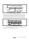
compare match occurs. Figure 12-9 shows an example of a procedure for setting up PWM mode.
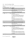
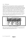
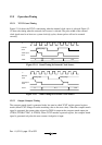
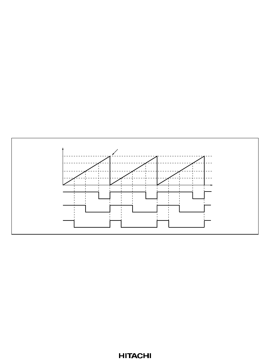
Figure 12-9 shows an example of operation in PWM mode. The output signals go to 1 and TCNT
is cleared at compare match A, and the output signals go to 0 at compare match B, C, and D
(TOB, TOC, and TOD = 1: initial output values are set to 1).
TCNT value
GRA
GRB
GRC
H'0000
FTIOB
FTIOC
FTIOD
Time
GRD
Counter cleared by compare match A
Figure 12-9 PWM Mode Example (1)
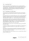
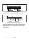
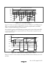
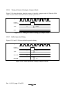
Figure 12-10 shows another example of operation in PWM mode. The output signals go to 0 and
TCNT is cleared at compare match A, and the output signals go to 1 at compare match B, C, and
D (TOB, TOC, and TOD = 0: initial output values are set to 1).