


Rev. 1.0, 07/01, page 203 of 372
14.5 Operation in Clocked Synchronous Mode
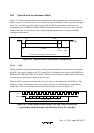
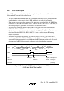
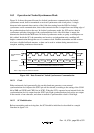
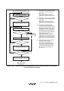
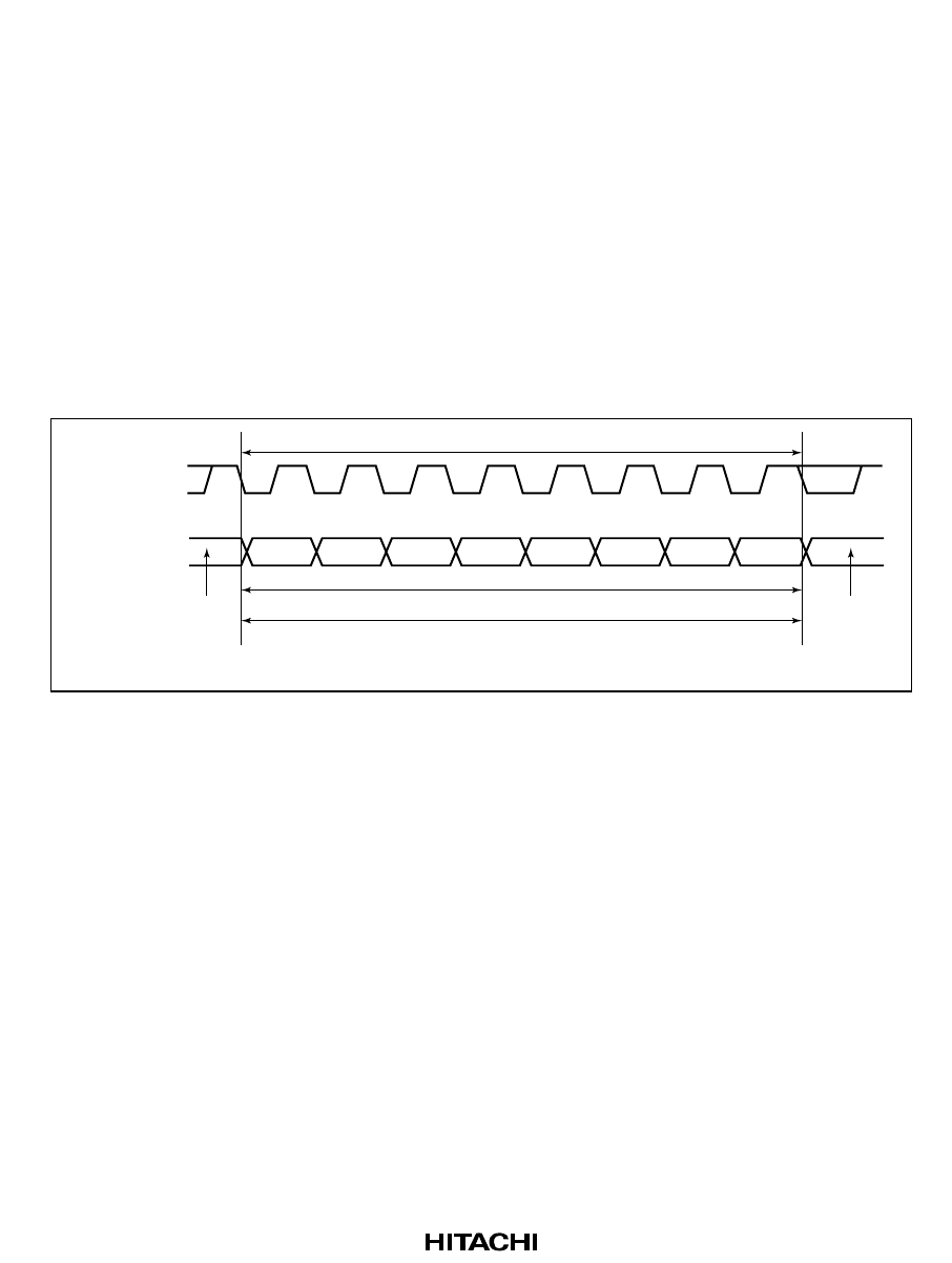
Figure 14-9 shows the general format for clocked synchronous communication. In clocked
synchronous mode, data is transmitted or received synchronous with clock pulses. A single
character in the transmit data consists of the 8-bit data starting from the LSB. In clocked
synchronous serial communication, data on the transmission line is output from one falling edge of
the synchronization clock to the next. In clocked synchronous mode, the SCI receives data in
synchronous with the rising edge of the synchronization clock. After 8-bit data is output, the
transmission line holds the MSB state. In clocked synchronous mode, no parity or multiprocessor
bit is added. Inside the SCI, the transmitter and receiver are independent units, enabling full-
duplex communication through the use of a common clock. Both the transmitter and the receiver
also have a double-buffered structure, so data can be read or written during transmission or
reception, enabling continuous data transfer.
LSB MSB
Don't care Don't care
One unit of transfer data (character or frame)
8-bit
Bit 0
Serial data
Synchronization
clock
Bit 1 Bit 3 Bit 4 Bit 5Bit 2 Bit 6 Bit 7
**
Note: * High except in continuous transfer
Figure 14-9 Data Format in Clocked Synchronous Communication
14.5.1 Clock
Either an internal clock generated by the on-chip baud rate generator or an external
synchronization clock input at the SCK3 pin can be selected, according to the setting of the COM
bit in SMR and CKE0 and CKE1 bits in SCR3. When the SCI is operated on an internal clock, the
synchronization clock is output from the SCK3 pin. Eight synchronization clock pulses are output
in the transfer of one character, and when no transfer is performed the clock is fixed high.
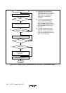
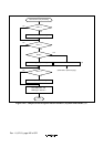
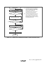
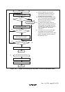
14.5.2 SCI Initialization
Before transmitting and receiving data, the SCI should be initialized as described in a sample
flowchart in figure 14-4.