


Rev. 1.0, 07/01, page 33 of 372
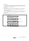
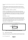
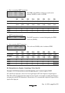
2.6 Basic Bus Cycle
CPU operation is synchronized by a system clock (ø) or a subclock (ø
SUB
). The period from a rising
edge of ø or ø
SUB
to the next rising edge is called one state. A bus cycle consists of two states or
three states. The cycle differs depending on whether access is to on-chip memory or to on-chip
peripheral modules.
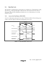
2.6.1 Access to On-Chip Memory (RAM, ROM)
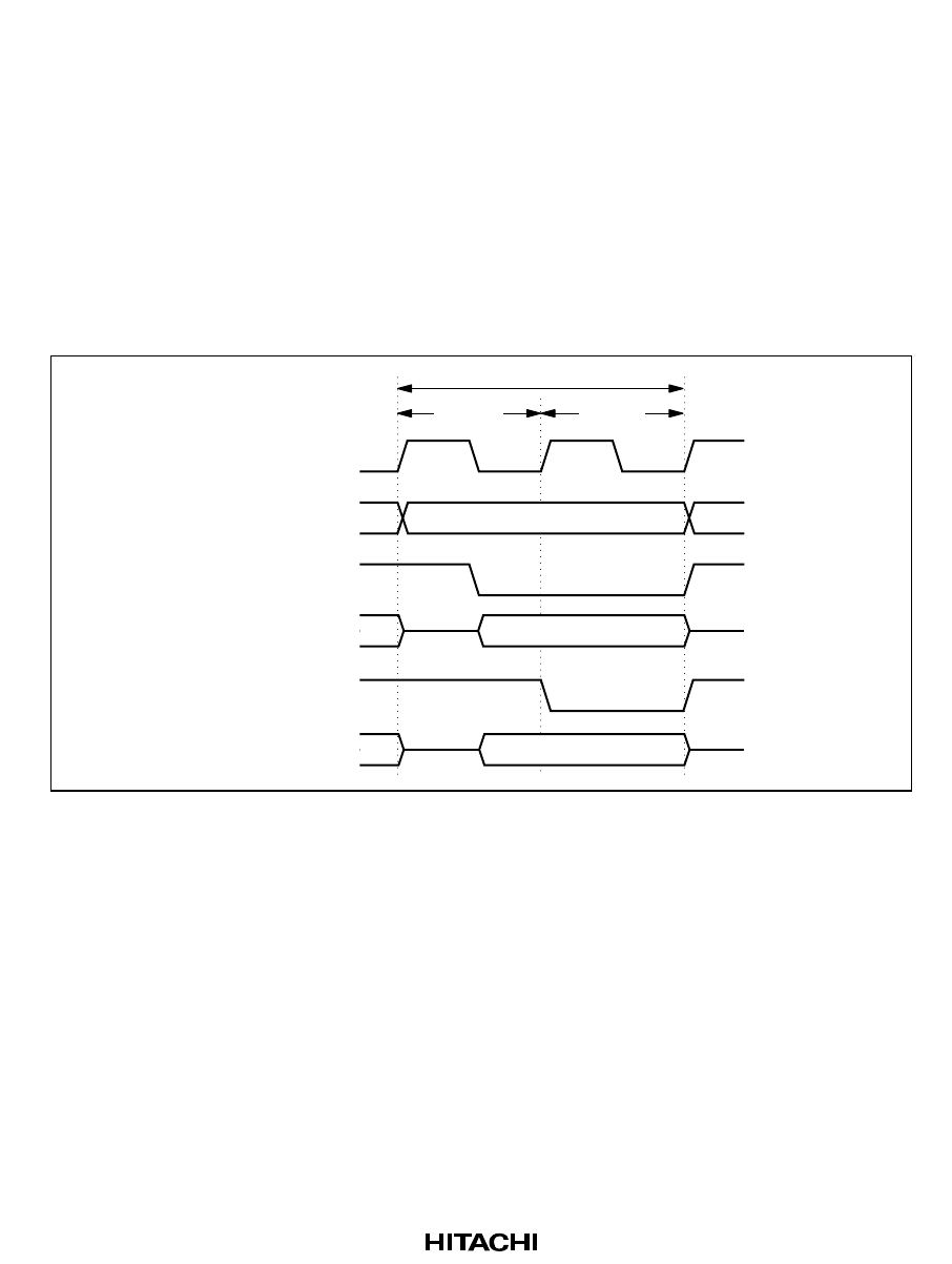
Access to on-chip memory takes place in two states. The data bus width is 16 bits, allowing access
in byte or word size. Figure 2-9 shows the on-chip memory access cycle.
T
1
state
Bus cycle
T
2
state
Internal address bus
Internal read signal
Internal data bus
(read access)
Internal write signal
Read data
Address
Write data
Internal data bus
(write access)
SUB
ø or ø
Figure 2-9 On-Chip Memory Access Cycle