


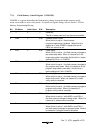
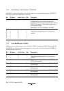
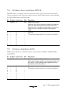
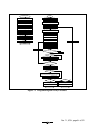
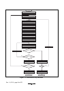
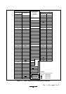
Rev. 71, 07/01, page 91 of 372
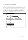
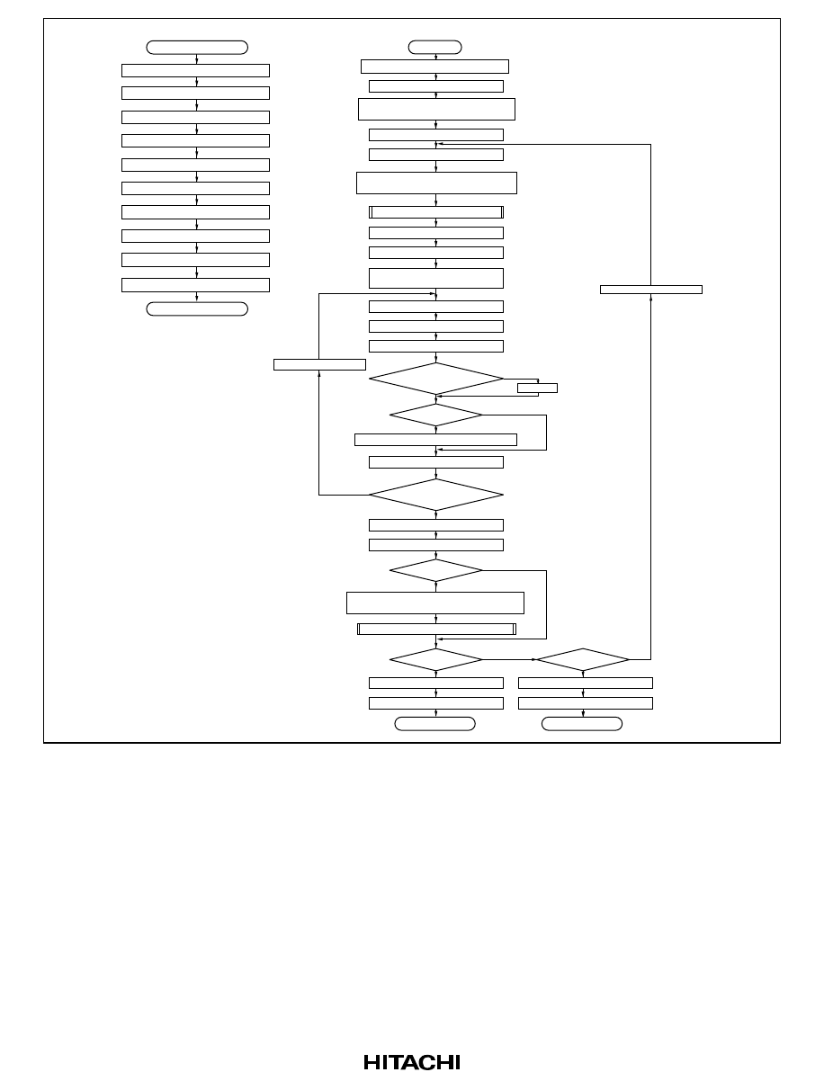
START
End of programming
Set SWE bit in FLMCR1 to 1
Write pulse application subroutine
Wait 1
µs
Apply Write Pulse
End Sub
Set PSU bit in FLMCR1 to 1
WDT enable
Disable WDT
Wait 50
µs
Set P bit in FLMCR1 to 1
Wait (Wait time=programming time)
Clear P bit in FLMCR1 to 0
Wait 5
µs
Clear PSU bit in FLMCR1 to 0
Wait 5
µs
n= 1
m= 0
No
No
No Yes
Yes
Yes
Yes
Wait 4
µs
Wait 2
µs
Wait 2
µs
Apply
Write Pulse
Set PV bit in FLMCR1 to 1
Set block start address as
verify address
H'FF dummy write to verify address
Read verify data
Verify data =
write data?
Reprogram data computation
Additional-programming data computation
Clear PV bit in FLMCR1 to 0
Clear SWE bit in FLMCR1 to 0
m = 1
m= 0 ?
Increment address
Programming failure
No
Clear SWE bit in FLMCR1 to 0
Wait 100
µs
No
Yes
n
≤
6?
No
Yes
n
≤
6 ?
Wait 100
µs
n ≤ 1000 ?
n ← n + 1
Write 128-byte data in RAM reprogram
data area consecutively to flash memory
Store 128-byte program data in program
data area and reprogram data area
Apply Write Pulse
Sub-Routine-Call
128-byte
data verification completed?
Successively write 128-byte data from additional-
programming data area in RAM to flash memory
Figure 7-3 Program/Program-Verify Flowchart