


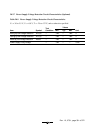

Rev. 1.0, 07/01, page 300 of 372
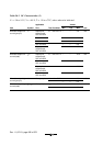
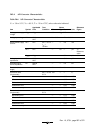
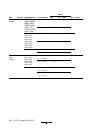
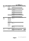
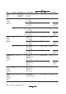
Test
Values
Item Symbol Condition Min Typ Max Unit
Erasing Wait time after SWE
bit setting
*
1
x 1 ——µs
Wait time after ESU
bit setting
*
1
y 100 — — µs
Wait time after E bit
setting
*
1
*
6
z 10 — 100 ms
Wait time after E bit clear
*
1
α
10——µs
Wait time after ESU bit clear
*
1
β
10——µs
Wait time after EV
bit setting
*
1
γ
20——µs
Wait time after dummy write
*
1
ε
2 ——µs
Wait time after EV bit clear
*
1
η
4 ——µs
Wait time after SWE
bit clear
*
1
θ
100 — — µs
Maximum number of
erases
*
1
*
6
*
7
N — — 120 Times
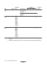
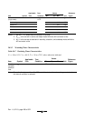
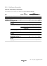
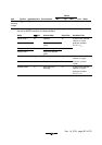
Notes: 1. Make the time settings in accordance with the program/erase algorithms.
2. The programming time for 128 bytes. (Indicates the total time for which the P bit in flash
memory control register 1 (FLMCR1) is set. The program-verify time is not included.)
3. The time required to erase one block. (Indicates the time for which the E bit in flash
memory control register 1 (FLMCR1) is set. The erase-verify time is not included.)
4. Programming time maximum value (t
P
(MAX)) = wait time after P bit setting (z) ×
maximum number of writes (N)
5. Set the maximum number of writes (N) according to the actual set values of z1, z2, and
z3, so that it does not exceed the programming time maximum value (t
P
(MAX)). The
wait time after P bit setting (z1, z2) should be changed as follows according to the value
of the number of writes (n).
Number of writes (n)
1 ≤ n ≤ 6 z1 = 30 µs
7 ≤ n ≤ 1000 z2 = 200 µs
6. Erase time maximum value (t
E
(max)) = wait time after E bit setting (z) × maximum
number of erases (N)
7. Set the maximum number of erases (N) according to the actual set value of (z), so that
it does not exceed the erase time maximum value (t
E
(max)).