


Rev. 1.0, 07/01, page 5 of 372
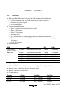
1.4 Pin Functions
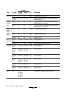
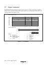
Table 1-1 Pin Functions
Pin No.
Type Symbol FP-64E
FP-64A
FP-48F I/O Functions
Power
source
V
CC
12 10 Input Power supply pin. Connect this pin to the
system power supply.
pins V
SS
9 7 Input Ground pin. Connect this pin to the system
power supply(0V).
AV
CC
3 1 Input Analog power supply pin for the A/D converter.
When the A/D converter is not used, connect
this pin to the system power supply.
V
CL
6 4 Input Internal step-down power supply pin. Connect
a capacitor of around 0.1µF between this pin
and the Vss pin for stabilization.
Clock
pins
OSC1 11 9 Input
OSC2 10 8 Output
These pins connect with crystal or ceramic
oscillator for the system clock, or can be used
to input an external clock.
See section 5, Clock Pulse Generators, for a
typical connection.
X1 5 3 Input
X2 4 2 Output
These pins connect with a 32.768 kHz crystal
oscillator for the subclock. See section 5, Clock
Pulse Generators, for a typical connection.
System
control
RES 7 5 Input Reset pin. When this driven low, the chip is
reset.
TEST 8 6 Input Test pin. Connect this pin to Vss.
Interrupt
pins
NMI 35 25 Input Non-maskable interrupt request input pin.
IRQ0 to
IRQ3
51 to 54 37 to 40 Input External interrupt request input pins. Can
select the rising or falling edge.
WKP0 to
WKP5
13, 14,
19 to 22
11 to 16 Input External interrupt request input pins. Can
select the rising or falling edge.
Timer A TMOW 23 17 Output This is an output pin for divided clocks.
Timer V TMOV 30 24 Output This is an output pin for waveforms generated
by the output compare function.
TMCIV 29 23 Input External event input pin.
TMRIV 28 22 Input Counter reset input pin.
TRGV 54 40 Input Counter start trigger input pin.