


Rev. 1.0, 07/01, page 37 of 372
Example 1 : Bit manipulation for the timer load register and timer counter
(Applicable for timer B and timer C, not for the series of this LSI.)
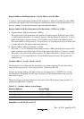
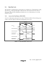
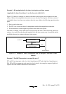
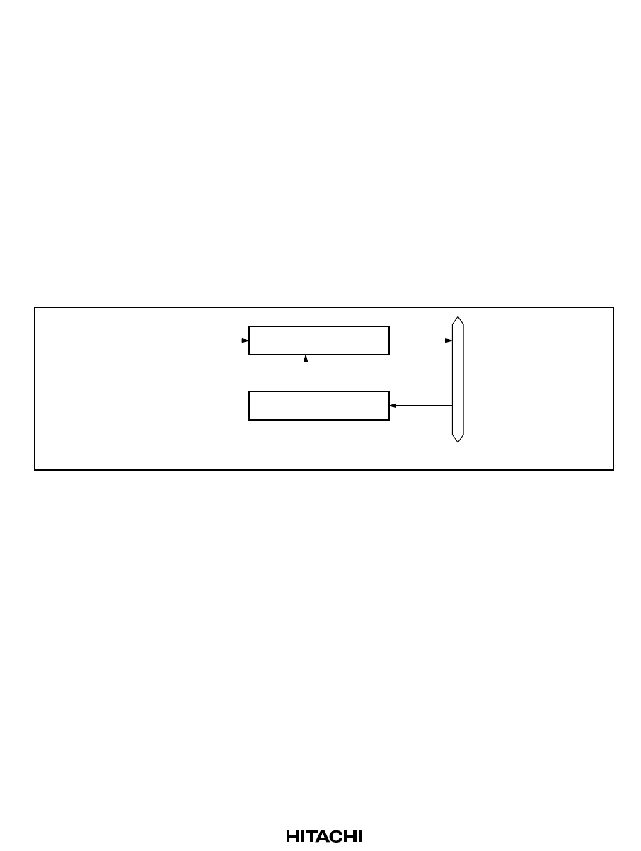
Figure 2-13 shows an example of a timer in which two timer registers are assigned to the same
address. When a bit manipulation instruction accesses the timer load register and timer counter of
a reloadable timer, since these two registers share the same address, the following operations takes
place.
1. Data is read in byte units.
2. The CPU sets or resets the bit to be manipulated with the bit manipulation instruction.
3. The written data is written again in byte units to the timer load register.
The timer is counting, so the value read is not necessarily the same as the value in the timer load
register. As a result, bits other than the intended bit in the timer counter may be modified and the
modified value may be written to the timer load register.
Read
Write
Count clock Timer counter
Timer load register
Reload
Internal data bus
Figure 2-13 Example of Timer Configuration with Two Registers Allocated to Same
Address
Example 2: The BSET instruction is executed for port 5.
P57 and P56 are input pins, with a low-level signal input at P57 and a high-level signal input at
P56. P55 to P50 are output pins and output low-level signals. An example to output a high-level
signal at P50 with a BSET instruction is shown below.