


Rev. 1.0, 07/01, page 167 of 372
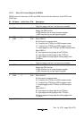
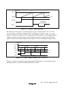
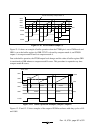
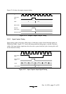
TCNT value
GRA
GRB
GRC
H'0000
FTIOB
FTIOC
FTIOD
Time
GRD
Counter cleared by compare match A
Figure 12-10 PWM Mode Example (2)
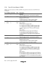
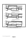
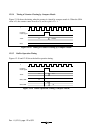
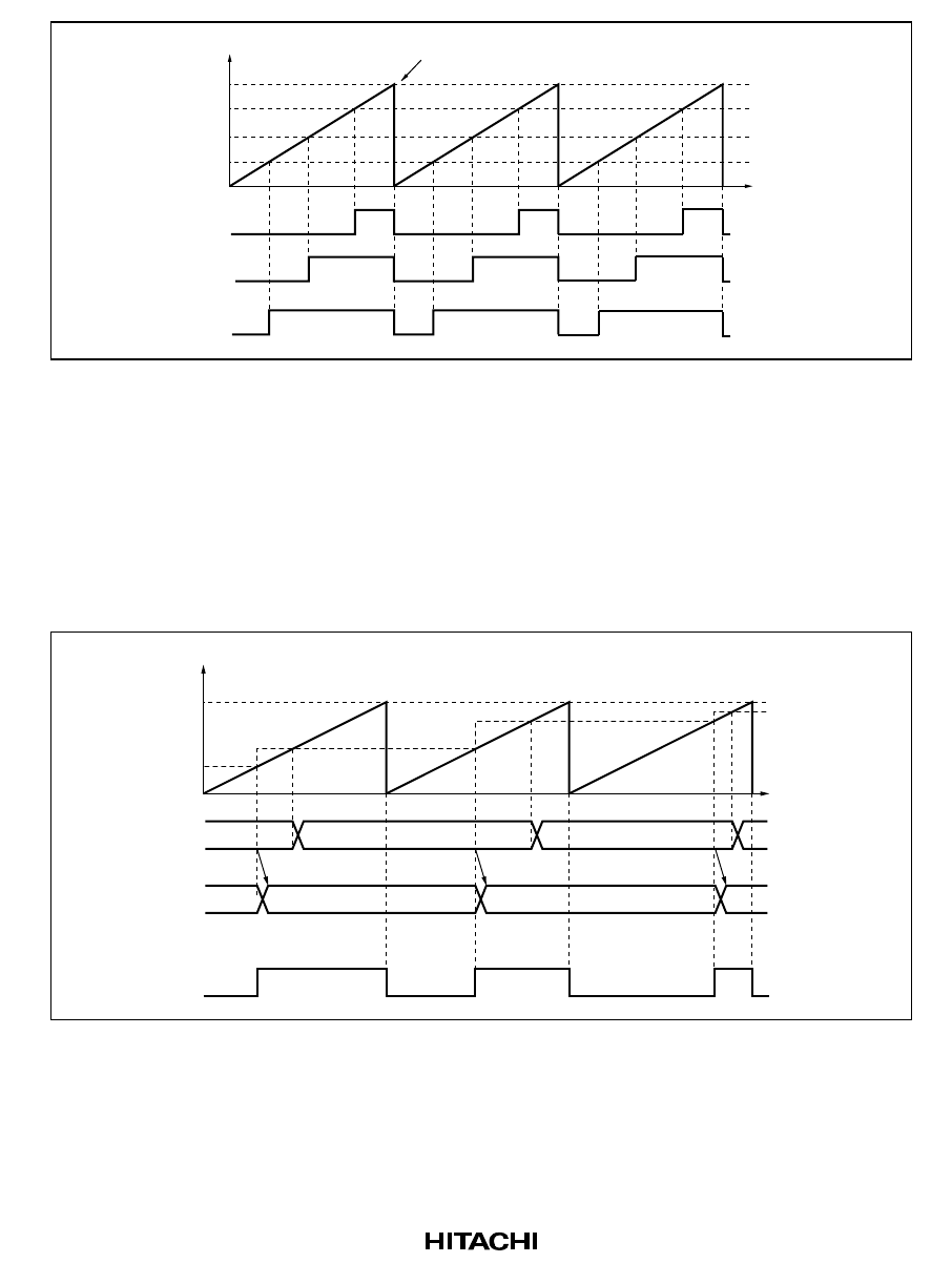
Figure 12-11 shows an example of buffer operation when the FTIOB pin is set to PWM mode and
GRD is set as the buffer register for GRB. TCNT is cleared by compare match A, and FTIOB
outputs 1 at compare match B and 0 at compare match A.
Due to the buffer operation, the FTIOB output level changes and the value of buffer register GRD
is transferred to GRB whenever compare match B occurs. This procedure is repeated every time
compare match B occurs.
TCNT value
GRA
H'0000
GRD
Time
GRB
H'0200 H'0520
FTIOB
H'0200
H'0450
H'0520
H'0450
GRB
H'0450 H'0520H'0200
Figure 12-11 Buffer Operation Example (Output Compare)
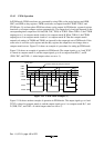
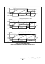
Figures 12-12 and 12-13 show examples of the output of PWM waveforms with duty cycles of 0%
and 100%.