


Rev. 1.0, 07/01, page 51 of 372
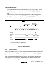
WKP5 to WKP0 Interrupts
WKP5 to WKP0 interrupts are requested by input signals to pins WKP5 to WKP0. These six
interrupts have the same vector addresses, and are detected individually by either rising edge
sensing or falling edge sensing, depending on the settings of bits WPEG5 to WPEG0 in
IEGR2.
When pins WKP5 to WKP0 are designated for interrupt input in PMR5 and the designated
signal edge is input, the corresponding bit in IWPR is set to 1, requesting the CPU of an
interrupt. These interrupts can be masked by setting bit IENWP in IENR1.
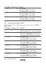
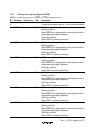
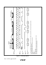
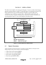
Vector fetch
ø
Internal
address bus
Internal read
signal
Internal write
signal
Internal data
bus (16 bits)
Internal
processing
Initial program
instruction prefetch
(1) Reset exception handling vector address (H'0000)
(2) Program start address
(3) Initial program instruction
(2) (3)
(2)
(1)
Reset cleared
Figure 3-1 Reset Sequence
3.4.2 Internal Interrupts
Each on-chip peripheral module has a flag to show the interrupt request status and the enable bit to
enable or disable the interrupt. For timer A interrupt requests and direct transfer interrupt requests
generated by execution of a SLEEP instruction, this function is included in IRR1 and IENR1.
When an on-chip peripheral module requests an interrupt, the corresponding interrupt request
status flag is set to 1, requesting the CPU of an interrupt. These interrupts can be masked by
writing 0 to clear the corresponding enable bit.