


Rev. 1.0, 07/01, page 294 of 372
Applicable
Values
Reference
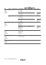
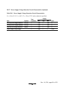
Item Symbol Pins Test Condition Min Typ Max Unit Figure
RES
pin low
width
t
REL
RES
At power-on and in
modes other than
those below
t
rc
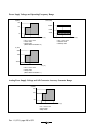
— — ms Figure 20-2
In active mode and
sleep mode
operation
10——t
cyc
Input pin high
width
t
IH
NMI
,
IRQ0
to
IRQ3
,
WKP0
to
WKP5
,
TMCIV,
TMRIV,
TRGV,
ADTRG
,
FTIOA to
FTIOD
2 ——t
cyc
t
subcyc
Figure 20-3
Input pin low
width
t
IL
NMI
,
IRQ0
to
IRQ3
,
WKP0
to
WKP5
,
TMCIV,
TMRIV,
TRGV,
ADTRG
,
FTIOA to
FTIOD
2 ——t
cyc
t
subcyc
Figure 20-3
Notes: 1. When an external clock is input, the minimum system clock oscillation frequency is
1.0 MHz.
2. Determined by MA2, MA1, MA0, SA1, and SA0 of system control register 2 (SYSCR2).