


Rev. 1.0, 07/01, page 196 of 372
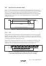
14.4.2 SCI Initialization
Before transmitting and receiving data, you should first clear the TE and RE bits in SCR3 to 0,
then initialize the SCI as described below. When the operating mode, or transfer format, is
changed for example, the TE and RE bits must be cleared to 0 before making the change using the
following procedure. When the TE bit is cleared to 0, the TDRE flag is set to 1. Note that clearing
the RE bit to 0 does not initialize the contents of the RDRF, PER, FER, and OER flags, or the
contents of RDR. When the external clock is used in asynchronous mode, the clock must be
supplied even during initialization.
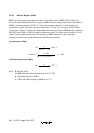
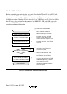
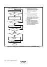
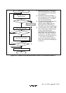
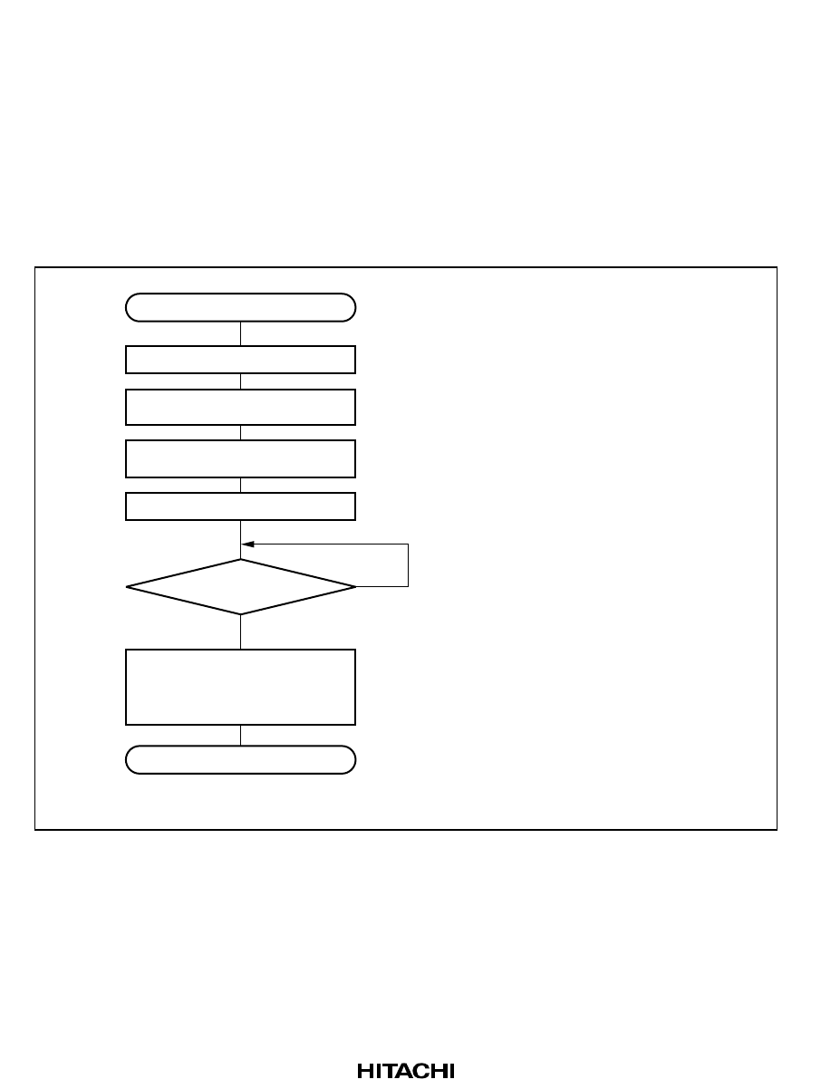
Wait
Start initialization
Set transfer data format in SMR
[1]
Set CKE1 and CKE0 bits in SCR3
No
Yes
Set value in BRR
Clear TE and RE bits in SCR3 to 0
[2]
[3]
Set TE or RE bit inSCR3 to 1, and
set RIE, TIE, TEIE,and MPIE bits
depending on necessity, For transmit
(TE=1), also set the TxD bit in PMR1.
[4]
1-bit interval elapsed?
[1] Set the clock selection in SCR3.
Be sure to clear bits RIE, TIE, TEIE, and
MPIE, and bits TE and RE, to 0.
When the clock output is selected in
asynchronous mode, clock is output
immediately after CKE1 and CKE0
settings are made. When the clock
output is selected at reception in clocked
asynchronous mode, clock is output
immediately after CKE1, CKE0, and RE
are set to 1.
[2] Set the data transfer format in SMR.
[3] Write a value corresponding to the bit
rate to BRR. Not necessary if an
external clock is used.
[4] Wait at least one bit interval, then set the
TE bit or RE bit in SCR3 to 1. RE
settings enable the RXD pin to be used.
For transmission, set the TXD bit in
PMR1 to 1 to enable the TXD output pin
to be used. Also set the RIE, TIE, TEIE,
and MPIE bits, depending on whether
interrupts are required. In asynchronous
mode, the bits are marked at
transmission and idled at reception to
wait for the start bit.
End of Initialization
Figure 14-4 Sample SCI Initialization Flowchart