


Rev. 1.0, 07/01, page 183 of 372
14.2 Input/Output Pins
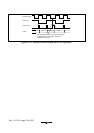
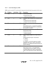
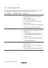
Table 14-1 shows the SCI pin configuration.
Table 14-1 Pin Configuration
Pin Name Abbrev. I/O Function
SCI clock SCK3 I/O SCI clock input/output
SCI receive data input RXD Input SCI receive data input
SCI transmit data output TXD Output SCI transmit data output
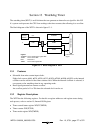
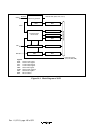
14.3 Register Descriptions
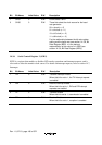
The SCI has the following registers for each channel. For details on register addresses and register
states during each process, refer to section 19, Internal I/O Register.
•
Receive Shift Register (RSR)
•
Receive Data Register (RDR)
•
Transmit Shift Register (TSR)
•
Transmit Data Register (TDR)
•
Serial Mode Register (SMR)
•
Serial Control Register3 (SCR3)
•
Serial Status Register (SSR)
•
Bit Rate Register (BRR)