


Rev. 1.0, 07/01, page 260 of 372
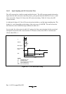
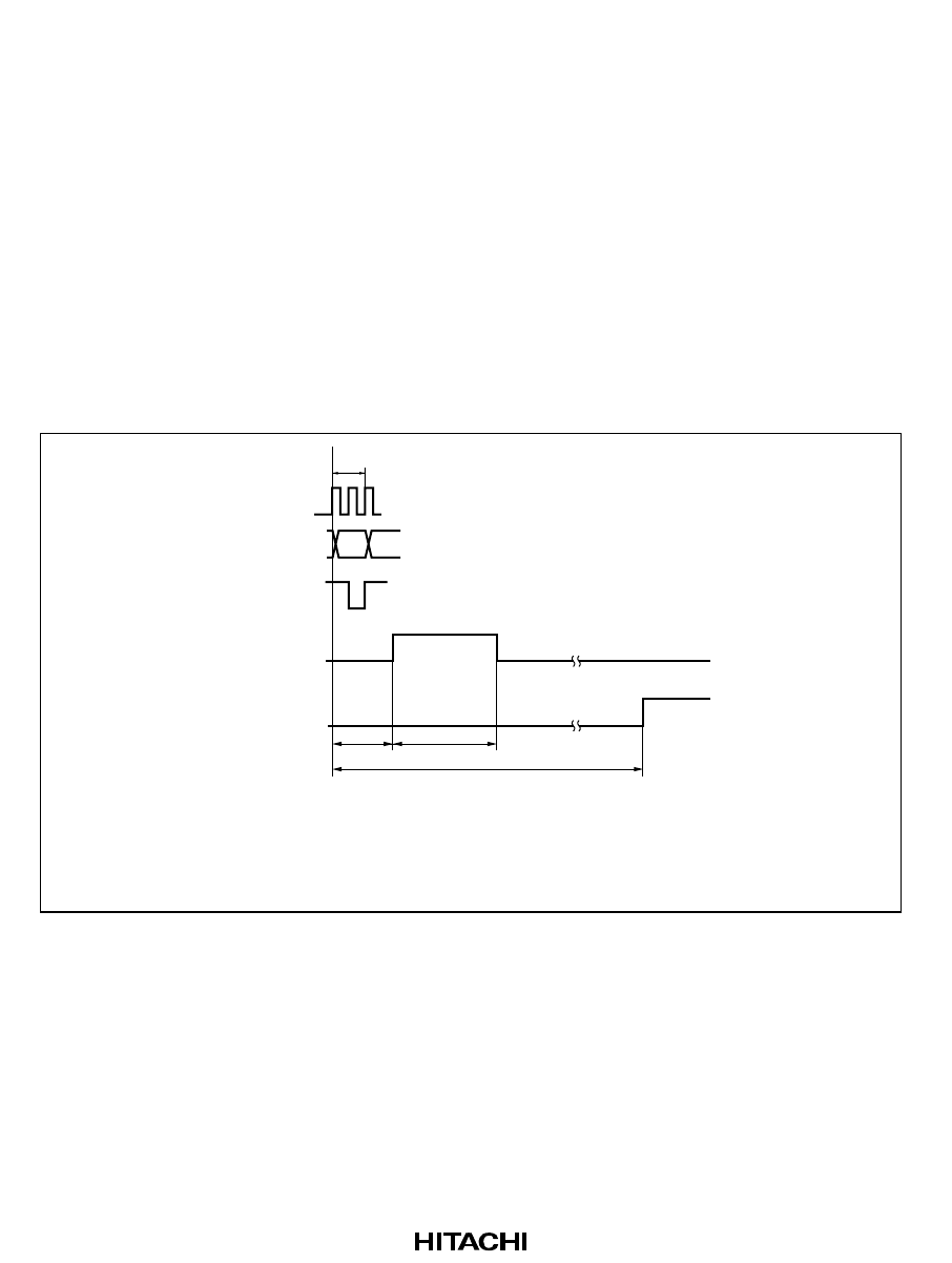
16.4.3 Input Sampling and A/D Conversion Time
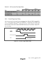
The A/D converter has a built-in sample-and-hold circuit. The A/D converter samples the analog
input when the A/D conversion start delay time (t
D
) has passed after the ADST bit is set to 1, then
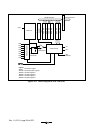
starts conversion. Figure 16-2 shows the A/D conversion timing. Table 16-3 shows the A/D
conversion time.
As indicated in figure 16-2, the A/D conversion time includes t
D
and the input sampling time. The
length of t
D
varies depending on the timing of the write access to ADCSR. The total conversion
time therefore varies within the ranges indicated in table 16-3.
In scan mode, the values given in table 16-3 apply to the first conversion time. In the second and
subsequent conversions, the conversion time is 128 states (fixed) when CKS = 0 and 66 states
(fixed) when CKS = 1.
(1)
(2)
t
D
t
SPL
t
CONV
ø
Address
Write signal
Input sampling
timing
ADF
Legend
(1) :
(2) :
t
D
:
t
SPL
:
t
CONV
:
ADCSR write cycle
ADCSR address
A/D conversion start delay time
Input sampling time
A/D conversion time
Figure 16-2 A/D Conversion Timing