


Rev. 1.0, 07/01, page 118 of 372
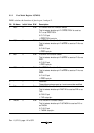
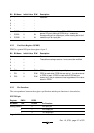
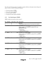
P21/RXD pin
Register SCR3 PCR2
Bit Name RE PCR21 Pin Function
Setting Value 0 0 P21 input pin
0 1 P21 output pin
1 X RXD input pin
Legend X:Don't care.
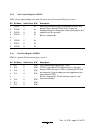
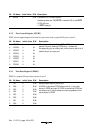
P20/SCK3 pin
Register SCR3 SMR PCR2
Bit Name CKE1 CKE0 COM PCR20 Pin Function
Setting Value 0 0 0 0 P20 input pin
0 0 0 1 P20 output pin
0 0 1 X SCK3 output pin
0 1 X X SCK3 output pin
1 X X X SCK3 input pin
Legend X:Don't care.
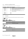
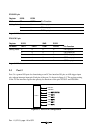
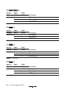
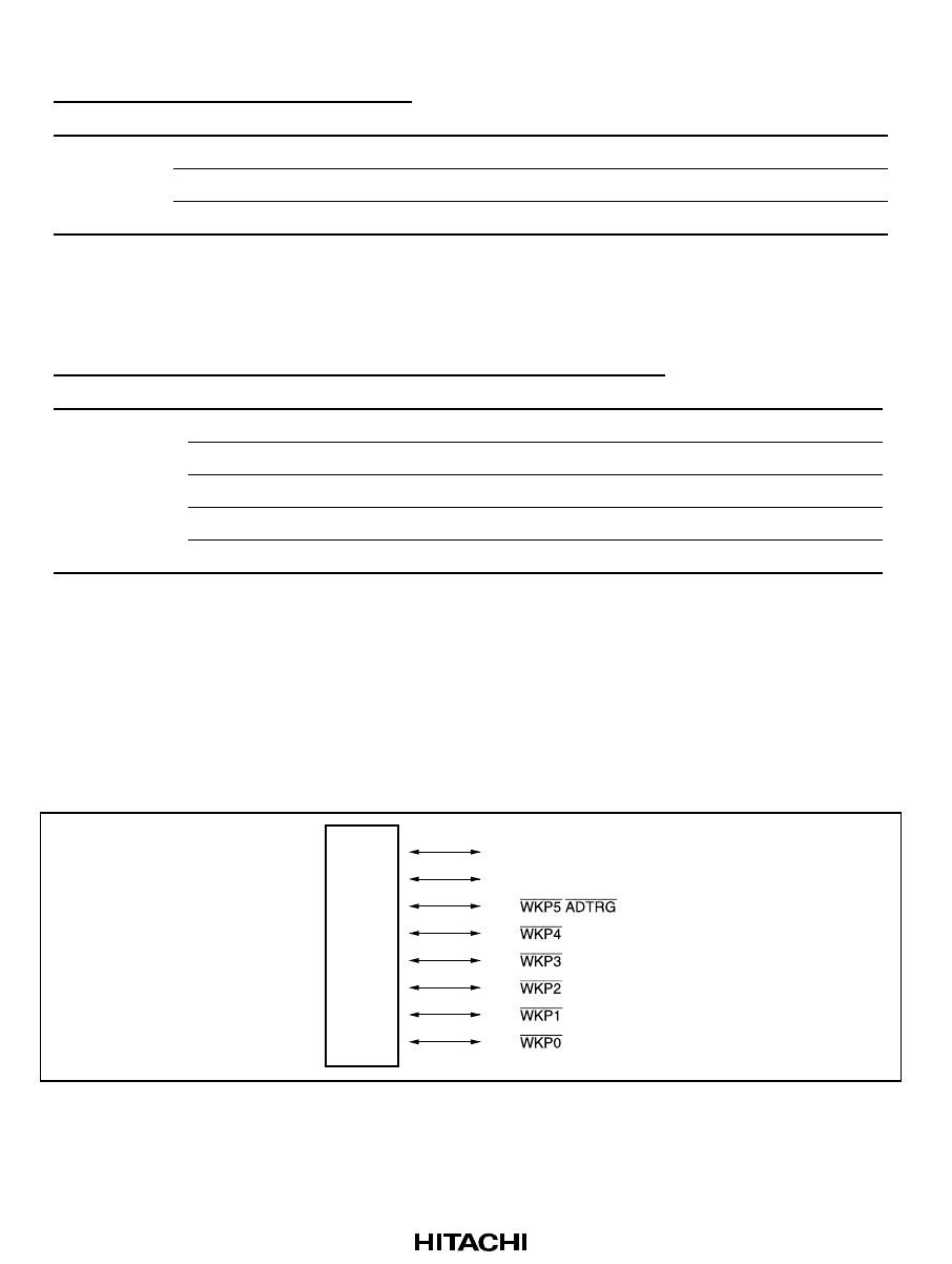
9.3 Port 5
Port 5 is a general I/O port also functioning as an I
2
C bus interface I/O pin, an A/D trigger input
pin, wakeup interrupt input pin. Each pin of the port 5 is shown in figure 9-3. The register setting
of the I
2
C bus interface register has priority for functions of the pins P57/SCL and P56/SDA.
P57/SCL
P56/SDA
P55/
/
P54/
P53/
P52/
P51/
P50/
Port 5
Figure 9-3 Port 5 Pin Configuration