


Rev. 1.0, 07/01, page 223 of 372
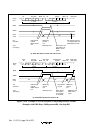
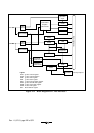
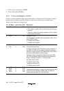
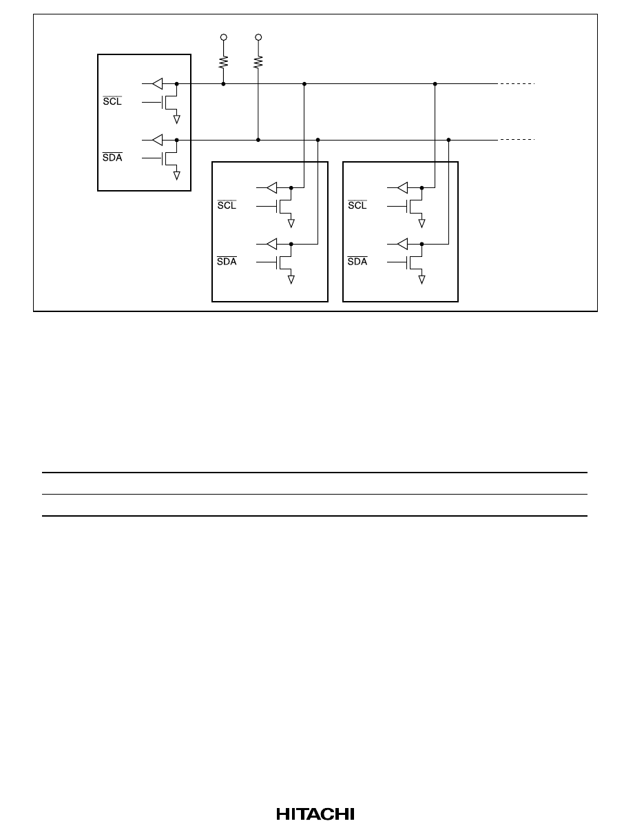
Vcc Vcc
SCL in
out
SCL
SDA in
out
SDA
SCL
(Master)
(Slave 1)
(Slave 2)
SDA
SCL in
out
SCL
SDA in
out
SDA
SCL in
out
SCL
SDA in
out
SDA
Figure 15-2 External Circuit Connections of I/O Pins
15.2 Input/Output Pins
Table 15-1 summarizes the input/output pins used by the I
2
C bus interface.
Table 15-1 I
2
C Bus Interface Pins
Name Abbreviation I/O Function
Serial clock SCL I/O IIC serial clock input/output
Serial data SDA I/O IIC serial data input/output
15.3 Register Descriptions
The I
2
C bus interface has the following registers. For details on register addresses and register
states during each processing, refer to section 19, Internal I/O Registers.
•
I
2
C bus control register 1 (ICCR1)
•
I
2
C bus control register 2 (ICCR2)
•
I
2
C bus mode register (ICMR)
•
I
2
C bus interrupt enable register (ICIER)
•
I
2
C bus status register (ICSR)
•
I
2
C bus slave address register (SAR)
•
I
2
C bus transmit data register (ICDRT)