


Rev. 1.0, 07/01, page 39 of 372
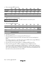
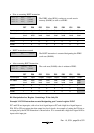
•
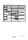
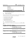
Prior to executing BSET instruction
MOV.B #80, R0L
MOV.B R0L, @RAM0
MOV.B R0L, @PDR5
The PDR5 value (H'80) is written to a work area in
memory (RAM0) as well as to PDR5.
P57 P56 P55 P54 P53 P52 P51 P50
Input/output Input Input Output Output Output Output Output Output
Pin state Low
level
High
level
Low
level
Low
level
Low
level
Low
level
Low
level
Low
level
PCR5 00111111
PDR5 10000000
RAM0 10000000
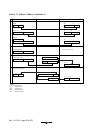
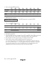
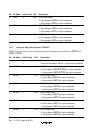
•
BSET instruction executed
BSET #0, @RAM0
The BSET instruction is executed designating the PDR5
work area (RAM0).
•
After executing BSET instruction
MOV.B @RAM0, R0L
MOV.B R0L, @PDR5
The work area (RAM0) value is written to PDR5.
P57 P56 P55 P54 P53 P52 P51 P50
Input/output Input Input Output Output Output Output Output Output
Pin state Low
level
High
level
Low
level
Low
level
Low
level
Low
level
Low
level
High
level
PCR5 00111111
PDR5 10000001
RAM0 10000001
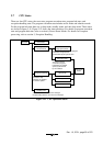
Bit Manipulation in a Register Containing a Write-Only Bit
Example 3: BCLR instruction executed designating port 5 control register PCR5
P57 and P56 are input pins, with a low-level signal input at P57 and a high-level signal input at
P56. P55 to P50 are output pins that output low-level signals. An example of setting the P50 pin as
an input pin by the BCLR instruction is shown below. It is assumed that a high-level signal will be
input to this input pin.